- About Us
- Solutions
- Industries
- Case Studies
- Resources
- Contact Us
Next Generation Lithography: A Lesser-Known Technology Behind the Evolution Semiconductor Chips

The advanced electronic materials and related technologies has a big impact on the increasing comfort of modern society is. Today, all the electronic tools that are essential for comfortable lifestyle including mobile phones, computers, laptops, sensors, and many more have one essential component in common, that is, semiconductor chip.
As these smart gadgets evolved over time, more and more advanced features were added to their services to make these devices more efficient and comfortable. Reduced semiconductor chip sizes and high throughputs make it possible for consumers to expect to pay less for smaller, faster, and more energy-efficient electronic gadgets that perform computational functions. One of the fundamental criteria for this advancement is semiconductor material patterning, which is accomplished by the lithography technology. 
Over time, the lithography technique has evolved into next generation lithography (NGL) technologies such as optical lithography, extreme ultraviolet (EUV) lithography, electron beam lithography (EBL), X-ray lithography, and ion beam lithography. In the article, a few of these advanced lithography techniques are discussed in detail, along with its impact on the evolution of semiconductor chips. But first, let’s understand what lithography technology is.
What is lithography?
Lithography is a key technology in the production of commercially viable microelectromechanical system (MEMS) devices in addition to being the driving force behind the semiconductor and IC industries. In the creation of nanoscience and engineering applications, and it is also utilised for prototype fabrication.
Several physical and chemical procedures must be carried out on a semiconductor substrate such as silicon to fabricate an integrated circuit (IC). The several steps involved in creating an IC can generally be divided into three groups: semiconductor doping, patterning, and film deposition. Transistors and their parts are connected and isolated using films that are both insulators (such as different types of silicon dioxide, silicon nitride, and others) and conductors (such as polysilicon, aluminium, and more recently copper). With the application of voltage, the conductivity of silicon can be altered due to selective doping of specific silicon areas.
Millions of transistors can be assembled and connected to construct the intricate circuitry of a contemporary MEMS device by building structures out of these diverse components. The creation of three-dimensional relief pictures on the substrate for later pattern transfer is known as lithography, and it is fundamental to all these techniques.
Next-Generation Lithography Techniques
1. X-Ray lithography: This lithography procedure uses a subset of nanolithography techniques, allowing for the patterning of transistors with more minute features. It transfers a geometric design from a mask to a substrate's light-sensitive chemical photoresist, or just "resist," using X-rays. The resulting design is then engraved into the substance beneath the photoresist through a succession of chemical processes.
The optical resolution of X-ray lithography can be increased to 15 nm by employing 1 nm illumination at short wavelengths. The proximity printing strategy is used to put this into practise. The method has advanced to the point where batch processing is possible.
The method's extension uses Fresnel diffraction of Near Field X-rays; a clear mask feature is "demagnified" by proximity to a wafer that is placed close to a "Critical Condition." This condition, which depends on both the wavelength and the size of the transparent mask feature, establishes the mask-to-wafer Gap.
Because no glasses are needed, the procedure is easy to process. The semiconductor industry originally considered this method as a potential contender for next-generation lithography, and it was successful in producing batches of microprocessors. Smaller feature sizes are possible thanks to X-rays' short wavelengths (below 1 nm), which get around optical lithography's diffraction restrictions. The refractive lenses are replaced with elementary collimating mirrors or diffractive lenses if the X-ray source is not collimated, as is the case with synchrotron radiation.
Advantages of X-ray lithography
• This technique can resolve diffraction issues
• Shorter wavelengths (0.1 - 10 nm)
• Smaller and more detailed features can be patterned
2. Electron Beam Lithography (EBL): In this method, a narrowly focused electron beam is scanned across a substrate's surface. In order to transfer the nanostructure into the substrate or later construct a device in a layer-by-layer fashion, electron beam lithography with ultra-high resolution (UHR) is typically employed at the very beginning of a multiple technique and multiple step process in a top-down approach.
EBL advantages
• Can write smaller features than X-ray lithography and photolithography; resolution is not constrained by diffraction.
• minimum feature is written on the nanoscale.
• The wafer is directly written with the pattern.
• employed to create prototypes and specialised gadgets
• It has quick turnaround times and uses an electron beam rather than a photon one.
3. Focused Ion beam lithography: Modern fabrication technology is focused on miniaturisation. Numerous current product components are getting smaller and smaller. The FIB offers the capacity for direct manufacturing of structures with feature sizes at or below 1 m because to the extremely short wavelength and extremely high energy density. As a result, creating high-quality microdevices or high-precision microstructures with the FIB has recently gained popularity.
In the semiconductor sector, the FIB has proved a potent tool, particularly for mask repair, device modification, failure analysis, and integrated circuit debugging. Ion beam direct write and ion beam projection are the two fundamental working modes created for these applications. The ion beams direct writing procedure, commonly referred to as FIB milling (FIBM), involves directly impinging the ion beam on the substrate to transfer patterns.
It is a sizable collection of microfabrication methods for creating different three-dimensional (3D) microstructures and devices out of a variety of materials by removing materials from a substrate. A collimated beam of ions passes through a stencil mask during the ion beam projection process, and the reduced image of the mask is then projected onto the substrate below. The focused ion beam lithography (FIBL) method of ion beam projection can be utilised as an alternative to traditional optical lithography.
Conclusion
A growing focus on cost-effective advanced technologies is encouraging the use of next-generation lithography techniques and materials to enhance the functionality and manufacturing process of semiconductor chips in several sectors.
Owing to the growing demand for cutting-edge microchips and semiconductors in smartphones and wearable technology, the next-generation lithography materials market is expected to grow at a healthy growth rate.
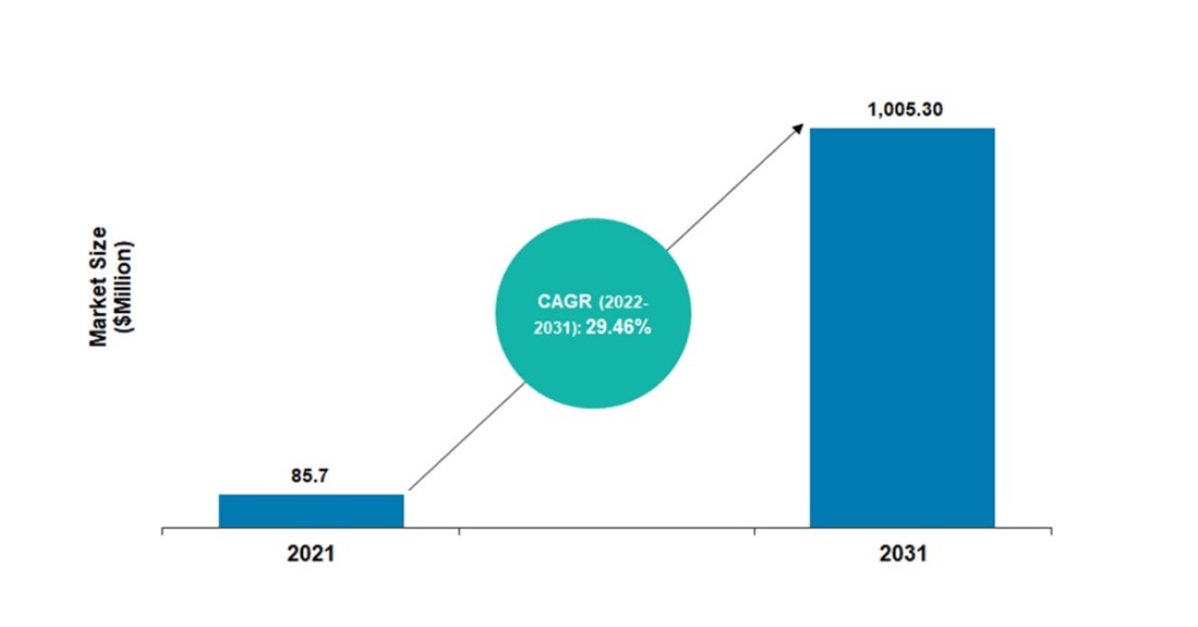
According to the BIS Research report, the global next-generation lithography materials market is projected to reach $1,005.3 million by 2031 from $85.7 million in 2021, growing at a CAGR of 29.46% during the forecast period 2022-2031.
Find more details on this report in this FREE sample
Interested to know more about the growing technologies in your industry vertical? Get the latest market studies and insights from BIS Research. Connect with us at hello@bisresearch.com to learn and understand more.

Get DeepTech Insights in your Mailbox!
Popular Posts
- Mycelium: A New Age Packaging Material
- Eco-Friendly Fabrics: The Rise of Castor Oil Biopolymers in the Textile Industry
- World’s First Single Piece 3D-Printed Rocket Engine is Ready to Thrust its First Flight
- Floating Data Center Market: Trends, Growth Drivers, and Future Prospects
- Precision Optics in the Next Decade: What to Expect and What's Possible
Recent Posts
- Metalens Market Outlook: Trends, Drivers, and Future Opportunities
- GPU Procurement Intelligence: GPUs Are Driving the Next Wave of AI Data Center Expansion
- GPU Deployment Boom: GPUs Are Powering the Next Generation of AI Data Centers
- GPU Operators: Leading the AI Infrastructure Race in U.S. Data Centers?
- BIS MarketIQ: The Intelligence Platform Powering AI GPU Infrastructure and Data Center Strategy
Posts by Topic
- Healthcare & Medical (83)
- Market Research Report (40)
- Agriculture & Food Tech (29)
- Advanced Materials & Chemicals (27)
- Automotive (27)
- Covid-19 (24)
- Aerospace defense (23)
- Robotics & UAV (23)
- Coronavirus (22)
- 3D Printing (20)
- Digital Technology (15)
- Electronics & Semiconductor (15)
- novel covid-19 (14)
- Electronic Cigarette (11)
- Precision Agriculture (11)
- novel coronavirus (10)
- Security & Surveillance (9)
- Artificial Intelligence (8)
- Webinar (8)
- corona virus (8)
- 3D Printing Market (7)
- BIS Research (7)
- precision agriculture market (7)
- BIS Research Webinar (6)
- Blockchain technology (6)
- Building Technologies & HVAC (6)
- Healthcare (6)
- Market Trends (6)
- UAV (6)
- Energy and sustainability (5)
- Waste Management & Envir Tech (5)
- covid19 (5)
- e-cigarette (5)
- electronic cigarette (5)
- precision medicine market (5)
- Agriculture (4)
- Automotive Cybersecurity (4)
- Computed Tomography (4)
- Electric Vehicles (4)
- Precision Farming (4)
- Unmanned Aerial Vehicles (4)
- precision medicine (4)
- precision medicine report (4)
- 3D Printer (3)
- 3D Printing Technology (3)
- Augmented Reality and Virtual Reality Market (3)
- Big Data (3)
- Biomanufacturing 4.0 (3)
- Counter-UAS Technology (3)
- Drones (3)
- EV Batteries (3)
- EV Battery Market (3)
- Healthcare Industry (3)
- Internet of Things (3)
- IoT in Agriculture Market (3)
- Market (3)
- Market Forecast (3)
- Plastics (3)
- SpaceTech (3)
- Surgical Procedure Volume Database (3)
- Surgical Robotics Market (3)
- automotive cybersecurity market (3)
- bis research blog (3)
- e liquid market forecast (3)
- e-cigarette market (3)
- electronic cigarette market (3)
- healthcare sector (3)
- market research report (3)
- noval corona virus (3)
- precision agriculture industry (3)
- precision agriculture report (3)
- precision farming market (3)
- precision medicine industry (3)
- space and aerospace (3)
- surgical robotics market growth (3)
- telemedicine (3)
- uav market forecast (3)
- 2016-2021 (2)
- 3D Printing Application Market (2)
- 3D Printing Market Analysis (2)
- 3D Printing Material (2)
- 3D Printing Material Market (2)
- 3D Printing Technology Market (2)
- 6G Technology (2)
- ADAS Market (2)
- Advanced Wound Dressing Market (2)
- Advancements in Augmented Reality (2)
- Aerospace (2)
- Agricultural Industry (2)
- Agricultural Sensors (2)
- Agriculture & Food (2)
- Agriculture Dealers Industry (2)
- Agriculture Dealers Market (2)
- Agriculture Drones and Robots Market (2)
- Agriculture Industry (2)
- Agriculture IoT (2)
- Agriculture Technology-as-a-Service Market (2)
- Augmented Reality (2)
- Automotive LiDAR Market (2)
- Automotive LiDAR Market Research (2)
- Automotive Market (2)
- Autonomous Vehicle (2)
- Autonomous Vehicle Market (2)
- Autonomous Vehicle Simulation Solutions Market (2)
- BVLOS drones (2)
- Battery (2)
- Blockchain Technology Market (2)
- CAD Market (2)
- CRISPR Technology Market (2)
- CRISPR Technology Market forecast (2)
- CRISPR Technology Market report (2)
- CRISPR Technology Market share (2)
- CRISPR Technology Market trends (2)
- CRISPR Technology Market value (2)
- CRISPR Technology Marketresearch (2)
- Carbon Negative (2)
- Cell and Gene Therapy (2)
- Cognitive Electronic Warfare System (2)
- Commercial Drones (2)
- Commercial Vehicles (2)
- Computer Aided Design Market (2)
- Consumer Printer (2)
- Crop Production (2)
- Cybersecurity (2)
- Defense Market (2)
- Diagnostic Imaging Market (2)
- Digital Agriculture Marketplace Market (2)
- Digital Technology Market (2)
- Disposable Protective Apparel (2)
- Drone (2)
- ENT Devices Market (2)
- EV Battery Pack Cooling System Industry (2)
- EV Battery Pack Cooling System Market (2)
- EV Battery Pack Cooling System Market Research (2)
- EV Battery industry (2)
- EV Battery report (2)
- Early Multicancer Detection (2)
- Electric Vehicle Battery industry (2)
- Electric Vehicles Battery Market (2)
- Emerging technology (2)
- Food Safety Testing Market (2)
- Food Safety Testing Services Market (2)
- Fuel Cells Market (2)
- Games of Skill Market (2)
- Global Augmented Reality Market (2)
- Global Augmented Reality and Virtual Reality Marke (2)
- Global Automotive Telematics Market (2)
- Global Automotive Telematics Market Report (2)
- Global Beacons Technology Market (2)
- Global Beacons Technology Market Analysis (2)
- Global Beacons Technology Market Analysis and Fore (2)
- Global Beacons Technology Market Forecast (2)
- Global Beacons Technology Market Research (2)
- Global Beacons Technology Market Share (2)
- Global CRISPR Technology Market (2)
- Global Carbon Nanotube Market Report (2)
- Global Carbon Nanotube Market Trends (2)
- Global Continuous Fiber Composites Market (2)
- Global Drone Market (2)
- Global EV Battery Market (2)
- Global Food Safety Testing Market (2)
- Global Food Safety Testing Market Analysis (2)
- Global Food Safety Testing Market Trends (2)
- Global Food Safety Testing Market growth (2)
- Global Industrial Microbiology industry analysis (2)
- Global Industrial Microbiology industry report (2)
- Global Intelligent Lighting Controls Market (2)
- Global Liquid Biopsy End User Market (2)
- Global Liquid Biopsy Market Share (2)
- Global Markets and Technologies for Food Safety (2)
- Global Medical Image Analytics Market (2)
- Global Next Generation Sequencing (2)
- Global Next Generation Sequencing Market Share (2)
- Global SLAM Technology Market (2)
- Global SLAM Technology Market Size (2)
- Global SLAM Technology Market Size by Country (2)
- Global SLAM Technology Market by Region (2)
- Global SLAM Technology Market for Robot (2)
- Global SLAM Technology Market for Robots by Commer (2)
- Global SLAM Technology Market for Robots by Househ (2)
- Global SLAM Technology Market for UAV (2)
- Global SLAM Technology Market forecast (2)
- Global SLAM Technology Market growth (2)
- Global SLAM Technology Market report (2)
- Global SLAM Technology Market research (2)
- Global SLAM Technology Market share (2)
- Global SLAM Technology Market trends (2)
- Global Surgical Robotics Market (2)
- Global UAV Sense and Avoid Systems Market (2)
- Global UAV market (2)
- Global Video Surveillance Market (2)
- Global iBeacon Market Size (2)
- Global liquid biopsy market (2)
- Global small caliber ammunition market (2)
- HVACR (2)
- HVACR Market (2)
- Healthcare Robots Trends (2)
- Heating Equipment Market (2)
- IOT in Oil and Gas (2)
- IVD Market (2)
- In-Space Economy (2)
- In-Vitro Fertilization Market (2)
- Indoor Vertical Farming (2)
- Industrial IoT Market (2)
- Industrial Microbiology Market (2)
- Industrial Microbiology Market Report (2)
- Industrial Microbiology Market forecast (2)
- Industrial Microbiology Market share (2)
- Industrial Microbiology Market size (2)
- Industrial Microbiology Market trends (2)
- Industrial microbiology (2)
- IoT (2)
- LED (2)
- LED Market (2)
- LiDAR Market (2)
- Lightweight Rooftop Solar PV Industry (2)
- Lightweight Rooftop Solar PV Market (2)
- Lightweight Rooftop Solar PV Report (2)
- Liquid Biopsy (2)
- Liquid Biopsy Market Size (2)
- Liquid Cooling Industry for Stationary BESS (2)
- Liquid Cooling Market for Stationary BESS (2)
- Liquid Cooling Report for Stationary BESS (2)
- Liquid biopsy market (2)
- Lithium-Ion Batteries (2)
- LoRaWAN (2)
- Low-Carbon Aluminum Industry (2)
- Low-Carbon Aluminum Market (2)
- Low-Carbon Aluminum Report (2)
- Machine learning (2)
- Market Growth (2)
- Medical Imaging Market (2)
- Mental Health (2)
- Microbiome Modulators Market (2)
- NGS Sample Preparation Market (2)
- NIPT (2)
- Nanocoatings Market (2)
- Neurostimulation Devices Market Share (2)
- Neurostimulation Devices Market growth (2)
- Neurostimulation Devices market (2)
- Non-Invasive Prenatal Testing Market (2)
- Powered Agriculture Equipment Market (2)
- Precision medicine market growth (2)
- Precision medicine market report (2)
- Precision medicine market size (2)
- Precision medicine market trends (2)
- Prefilled Syringes Market (2)
- Radiation Dose Management (2)
- Remote Drone Identification System Market Size (2)
- Robotics and Imaging (2)
- SLAM Technology for Augmented Reality (2)
- SLAM Technology for Autonomous Vehicles (2)
- SLAM Technology for Robots (2)
- SLAM Technology for UAV (2)
- SLV Market (2)
- Satellite Spectrum Monitoring (2)
- Satellite Spectrum Monitoring Market (2)
- Satellites (2)
- Sensor (2)
- Small Launch Vehicle Market (2)
- Small Modular Reactor Market (2)
- Small Satellite Market Forecast (2)
- Smart Lighting Market (2)
- Surgical Robotics (2)
- Surgical Robotics Market trends (2)
- Surgical Robotics industry (2)
- Surgical Robotics report (2)
- Sustainable Future (2)
- Sustainable Space (2)
- Switchgear Monitoring System Market (2)
- Switchgear Monitoring System Market size (2)
- UAVs (2)
- UK E cigarette market (2)
- Unmanned Aerial Vehicles Market (2)
- VTOL Aircraft Market (2)
- Vertical Farming (2)
- Wearable Technology (2)
- Wound Cleanser Products Market (2)
- advanced electronic materials (2)
- anti money laundering software market size (2)
- applications of crispr technology (2)
- automotive sector (2)
- beacon market research (2)
- beacon market size (2)
- beacon marketing solutions (2)
- beacon technology (2)
- beacon technology market research (2)
- beacon technology market size (2)
- biometric identification market (2)
- bluetooth beacon technology (2)
- cancer treatment (2)
- cannabis market in North America (2)
- corona (2)
- crispr cas technology (2)
- crispr cas9 technology (2)
- crispr gene technology (2)
- crispr news (2)
- crispr technology (2)
- crispr technology companies (2)
- data centers (2)
- data mining (2)
- defense industry (2)
- defense outlook (2)
- drone industry (2)
- drones market research (2)
- drug discovery (2)
- e cigarette market reports (2)
- e liquid market study (2)
- e vapor (2)
- eddystone beacon technology market size (2)
- electric propulsion (2)
- electric vehicle (2)
- electric vehicle industry (2)
- electronic cigarette market report (2)
- european e liquid market (2)
- european e liquid market reports (2)
- fleet management market (2)
- food pathogen testing market size (2)
- food safety market size (2)
- global food safety testing market size (2)
- global healthcare robotics market (2)
- global positioning systems (2)
- green hydrogen technology (2)
- healthcare trends (2)
- high acuity information systems (2)
- hvac market forecast (2)
- hvac market report (2)
- ibeacon for real estate (2)
- iot security market analysis (2)
- iot security market forecast (2)
- liquid biopsy market report (2)
- market size (2)
- medical imaging (2)
- medical robotics industry growth (2)
- micro mobility market (2)
- minimally invasive surgical systems market (2)
- next generation sequencing market (2)
- novel corona virus (2)
- pathogen testing market (2)
- pollution (2)
- robotic surgery market (2)
- robotic surgery market size (2)
- satellite imaging (2)
- small satellite launch market (2)
- space technology (2)
- stratasys (2)
- surgical procedure volume data (2)
- surgical robots market (2)
- uav market report (2)
- unmanned aerial vehicle market (2)
- vape (2)
- vapor (2)
- ventilators (2)
- video surveillance market forecast (2)
- wearable electronics (2)
- what is crispr technology (2)
- world environment day (2)
- 2019 AI Trends (1)
- 3D Cell Culture (1)
- 3D Printed Gown (1)
- 3D Printing Market for Aerospace (1)
- 3D Printing Market for Aerospace Industry by Mater (1)
- 3D Printing Market for Aerospace Industry by Regio (1)
- 3D Printing Market for Automotive (1)
- 3D Printing Market for Automotive Industry by Mate (1)
- 3D Printing Market for Automotive Industry by Regi (1)
- 3D Printing Material Market Forecast (1)
- 3D Printing Materials Market (1)
- 3D Printing Materials Market Research (1)
- 3D Printing Plastic Market (1)
- 3D Printing Plastic and Photopolymer Material Mark (1)
- 3D Printing Software (1)
- 3D Printing Software and Services Market (1)
- 3D Printing Technologies (1)
- 3D Printing Technology Industry (1)
- 3D Printing Technology report (1)
- 3D Printing in Food Industry (1)
- 3D Protein Structure (1)
- 3D printing in Fashion (1)
- 3D printing market report (1)
- 3D printing materials Aerospace (1)
- 3D printing materials Automotive (1)
- 3D printing or additive manufacturing (1)
- 3D printing software market (1)
- 3D printing technology aerospace (1)
- 3D printing technology automotive (1)
- 3D-Printed Rocket Engine (1)
- 3DP (1)
- 3DP Market (1)
- 3DP Meterials Market (1)
- 3DP Technology (1)
- 3d (1)
- 3d Printer in Medical (1)
- 3d bioprinting market (1)
- 3d bioprinting market report (1)
- 3d bioprinting market size (1)
- 3d printed gun (1)
- 3d printing in automotive (1)
- 3d printing in dental (1)
- 3d printing market research (1)
- 3d printing market share (1)
- 3d printing market size (1)
- 3d printing market trends (1)
- 3d printing use case (1)
- 4d printing (1)
- 5G Industry (1)
- 5G Infrastructure (1)
- 5G Infrastructure Industry (1)
- 5G Infrastructure Market (1)
- 5G Infrastructure Market Analysis (1)
- 5G Infrastructure Market By Spectrum Type (1)
- 5G Infrastructure Market Forecast (1)
- 5G Infrastructure Market Growth (1)
- 5G Infrastructure Market Research Report (1)
- 5G Infrastructure Market Share (1)
- 5G Infrastructure Market Trends (1)
- 5G Infrastructure Market by Application (1)
- 5G Infrastructure Market by Region (1)
- 5G Infrastructure Market key[players (1)
- 5G Infrastructure Report (1)
- 5G Market (1)
- 5G Network Industry (1)
- 5G Network Market (1)
- 5G Network Market Study (1)
- 5G Network Report (1)
- 5G Report (1)
- 5G Satellite (1)
- 5G Technology Forecast (1)
- 5G Technology Industry (1)
- 5G Technology Market (1)
- 5G Technology Market Research (1)
- 5G Technology Market Study (1)
- 5G Technology Market Trends (1)
- 5G Technology Report (1)
- 5G Technology Share (1)
- 5G technologies (1)
- 5GNetwork Market Research (1)
- 5g Market Share (1)
- 5g Market Share Analysis (1)
- 5g Market Study (1)
- 5g Market Trends (1)
- 5g market forecast (1)
- ABS (1)
- ADAS (1)
- ADAS Commercial Vehicles Market (1)
- ADAS Commercial Vehicles Market Forecast (1)
- ADAS Market Size by Commercial Vehicles Market (1)
- ADAS Vehicle Market (1)
- ADAS market size (1)
- AGEYE (1)
- AGV (1)
- AGV Market (1)
- AGV Market Analysis (1)
- AGV Market Outlook (1)
- AGV Market Study (1)
- AI Applications (1)
- AI Healthcare (1)
- AI Market Reports (1)
- AI in 2019 (1)
- AI in Healthcare Market (1)
- AI in Healthcare Robotics (1)
- AI in Medical Imaging (1)
- AI in Operating Room Market (1)
- AI in cybersecurity (1)
- AI systems (1)
- AI-Enabled Medical Imaging (1)
- AI-Enabled Medical Imaging Solutions Market (1)
- AI-Powered Cybersecurity (1)
- AI-based ECG technology (1)
- AIP System (1)
- AIP systems for submarines (1)
- AIP technology (1)
- APAC Air Purifier Market (1)
- APAC Air Purifier Market analysis (1)
- APAC Air Purifier Market growth (1)
- APAC Air Purifier Market report (1)
- APAC Air Purifier Market research report (1)
- APAC Air Purifier Market share (1)
- APAC Air Purifier industry analysis (1)
- APAC Air Purifiers Player Share Analysis (1)
- APAC Autonomous Vehicle Market (1)
- APAC E-cigarette Market (1)
- APAC E-cigarette Market Forecast (1)
- APAC E-cigarette Market Survey (1)
- APAC E-cigarette Market Trends (1)
- APAC E-cigarette Report (1)
- APAC E-liquid Market (1)
- APAC E-liquid Market Forecast (1)
- APAC E-liquid Market Report (1)
- APAC E-liquid Market Size (1)
- APAC E-liquid Market Study (1)
- APAC Fiber Optic Cable Industry (1)
- APAC Fiber Optic Cable Market (1)
- APAC Fiber Optic Cable Report (1)
- APAC Precision Farming Market (1)
- APAC Space Carbon Composite Fiber Market (1)
- APAC Space Carbon Fiber Composite Industry (1)
- APAC Space Carbon Fiber Composite Report (1)
- APAC TJA Systems Market (1)
- APAC Traffic Jam Assist Systems Market (1)
- APAC microgrid market (1)
- AR (1)
- AR & MR Market Research (1)
- AR Market (1)
- AR and VR Market (1)
- AVping (1)
- Accelermeter (1)
- Acid Metal Complex Dyes Industry (1)
- Acid Metal Complex Dyes Market (1)
- Acid Metal Complex Dyes Report (1)
- Acquistion (1)
- Actuators Market (1)
- Actuators Market Analysis (1)
- Adaptive Lighting Market (1)
- Adaptive Lighting Market Analysis (1)
- Adaptive Lighting Systems (1)
- Added by Bhavya (1)
- Additive manufacturing application market (1)
- Addressable Market Size and Growth Potential (1)
- Adjuvant agriculture (1)
- Advance Energy Storage Market (1)
- Advance Energy Storage Market Trends (1)
- Advanced Dental Digital Solutions Market (1)
- Advanced Dental Robotics Solutions Market (1)
- Advanced Driver Assistance System Market (1)
- Advanced Energy Storage Market Report (1)
- Advanced Energy Storage Market Study (1)
- Advanced Message Queuing Protocol (1)
- Advanced Space Composites Industry (1)
- Advanced Space Composites Market (1)
- Advanced Space Composites Report (1)
- Advanced Traffic Management System (1)
- Advanced Transportation Pricing System (1)
- Advanced Traveler Information System (1)
- Advanced Wound Care Market Analysis (1)
- Advanced Wound Care Market Report (1)
- Advanced Wound Care Market Size (1)
- Advanced Wound Care Market Study (1)
- Advanced Wound Care Market Survey (1)
- Advanced Wound Dressing Industry (1)
- Advanced Wound Dressing Report (1)
- Advanced directed energy weapons (1)
- Advanced propane dehydrogenation (1)
- Advances in UAV Communications (1)
- Advancing Precision Medicine (1)
- AeroFarms (1)
- Aeroponics (1)
- Aerospace 3D Printing Industry (1)
- Aerospace 3D Printing Market (1)
- Aerospace 3D Printing Market Forecast (1)
- Aerospace 3D Printing Market Share (1)
- Aerospace 3D Printing Market Trends (1)
- Aerospace 3D Printing Report (1)
- Agnikul Cosmos (1)
- Agri-Drones Market (1)
- AgriDigital (1)
- Agribusinesses (1)
- Agricultural Films Market (1)
- Agricultural Films Market Research Forecast (1)
- Agricultural Films Market Research Report (1)
- Agricultural Films Market Share (1)
- Agricultural Films Market Size (1)
- Agricultural Films Market forecast (1)
- Agricultural Robots Market (1)
- Agricultural Robots Market Analysis (1)
- Agricultural Robots Market Research (1)
- Agricultural Robots Market Trends (1)
- Agricultural Sensors Market (1)
- Agricultural Sprayers Industry (1)
- Agricultural Sprayers Market (1)
- Agricultural Sprayers Report (1)
- Agricultural Tractor Industry (1)
- Agricultural Tractor Market (1)
- Agricultural Tractor Report (1)
- Agricultural adjuvants market (1)
- Agriculture Autonomous Retrofit Industry (1)
- Agriculture Autonomous Retrofit Market (1)
- Agriculture Autonomous Retrofit Report (1)
- Agriculture Autonomous Robots Industry (1)
- Agriculture Autonomous Robots Market (1)
- Agriculture Autonomous Robots Market Report (1)
- Agriculture Autonomous Robots Market Size (1)
- Agriculture Carbon Sequestration Industry (1)
- Agriculture Carbon Sequestration Market (1)
- Agriculture Carbon Sequestration Report (1)
- Agriculture Customer Segmentation Industry (1)
- Agriculture Customer Segmentation Market (1)
- Agriculture Customer Segmentation Report (1)
- Agriculture Dealers Market Report (1)
- Agriculture Dealers Report (1)
- Agriculture Drones (1)
- Agriculture Equipment Industry (1)
- Agriculture Imaging Sensor Industry (1)
- Agriculture Imaging Sensor Market (1)
- Agriculture Imaging Sensor Market Report (1)
- Agriculture Internet of Things Technology Market (1)
- Agriculture Market (1)
- Agriculture Market Report (1)
- Agriculture Sensor Technology (1)
- Agriculture Sensors (1)
- Agriculture Technology-as-a-Service (1)
- Agriculture Tractor Market (1)
- Agriculture technologies (1)
- Agriculture technology (1)
- Agriculture technology Market (1)
- Agrigenomics Market (1)
- Agritech (1)
- Air Cooling (1)
- Air Purifier Market (1)
- Air Purifier Market report (1)
- Airborne LiDAR Services Market (1)
- Airborne LiDAR System Market (1)
- Airborne LiDAR System Market forecast (1)
- Airborne LiDAR System Market gorwth (1)
- Airborne LiDAR System Market report (1)
- Airborne LiDAR System Market scop (1)
- Airborne LiDAR System Market share (1)
- Airborne LiDAR System Market size (1)
- Airborne LiDAR System Market trends (1)
- Airborne LiDAR System Market value (1)
- Aircraft Landing Gear Market Forecast (1)
- Aircraft Landing Gear Market Research (1)
- Algae Biofuel Industry (1)
- Algae Biofuel Market (1)
- Algae Biofuel Report (1)
- Alkaline Water Electrolysis (1)
- Ambulatory Centers (1)
- Ambulatory surgery centers (1)
- America (1)
- America HVACR Market (1)
- America HVACR Market Research (1)
- Americas HVACR Market (1)
- Americas HVACR Market Report (1)
- Americas Heating Ventilation Air Conditioning and (1)
- Americas Prefabricated Steel Building Market Analy (1)
- Analysis & Forecast (1)
- Analyst brief (1)
- Analysts Note (1)
- Android Auto (1)
- Animal Health Monitoring & Comfort Systems (1)
- Animal genetics (1)
- Anti Fingerprint Industry Analysis (1)
- Anti Fingerprint Market Forecast (1)
- Anti Fingerprint Market Share (1)
- Anti Fingerprint Market Trends (1)
- Anti Fingerprint coatings Industry (1)
- Anti Fingerprint coatings Market (1)
- Anti Fingerprint coatings Report (1)
- Anti Reflective Industry Analysis (1)
- Anti Reflective Market Forecast (1)
- Anti Reflective Market Growth (1)
- Anti Reflective Market Share (1)
- Anti Reflective and Anti Fingerprint Industry (1)
- Anti Reflective and Anti Fingerprint Market (1)
- Anti Reflective and Anti Fingerprint Report (1)
- Anti-Aging Devices Market (1)
- Anti-Aging Devices Market Analysis (1)
- Anti-Aging Devices Market Outlook (1)
- Anti-Aging Devices Market Report (1)
- Anti-Aging Devices Market Share (1)
- Anti-Aging Devices Market Size (1)
- Anti-Aging Devices Market forecast (1)
- Anti-Drone Market (1)
- Anti-Money Laundering Software Market (1)
- Anti-Money Laundering Software market share (1)
- Antibody Conjugate Oligonucleotide market (1)
- Antistatic agents (1)
- Application of Circulating cfDNA (1)
- Aquaponics (1)
- Aquaponics and Hydroponics market forecast (1)
- Aquaponics and Hydroponics market growth (1)
- Aquaponics and Hydroponics market industry analysi (1)
- Aquaponics and Hydroponics market research (1)
- Aquaponics and Hydroponics market share (1)
- Aquaponics and Hydroponics market trend (1)
- Aquaponics and Hydroponics market value (1)
- Aquaponics system market (1)
- Aqueous Zinc Flow Battery Industry (1)
- Aqueous Zinc Flow Battery Market (1)
- Aqueous Zinc Flow Battery Report (1)
- Architecture of Clinical Decision Support System (1)
- Artificial Intelligence Market in Healthcare (1)
- Artificial Intelligence Medical Device Industry (1)
- Artificial Intelligence Medical Device Market (1)
- Artificial Intelligence in Healthcare (1)
- Artificial Intelligence in Healthcare Robotics (1)
- Artificial Intelligence in Medical Imaging (1)
- Artificial Intelligence in Real Time Monitoring (1)
- Artificial Organs Industry Analysis (1)
- Artificial Organs Market (1)
- Artificial Organs Market Forecast (1)
- Artificial Organs Market Growth (1)
- Artificial Organs Market Report (1)
- Artificial Organs Market Research (1)
- Artificial Organs Market Share (1)
- Artificial Organs Market Trends (1)
- Artificial Organs Market by Organ Type (1)
- Artificial Organs Market by Region (1)
- Artificial Organs Market by Technology (1)
- Artificial Organs industry (1)
- Artificial Organs report (1)
- Artillery (1)
- Aseptic Connectors Market (1)
- Aseptic Pharma Processing (1)
- Aseptic Pharma Processing Market (1)
- Asia Pacific E-cigarette Market (1)
- Asia Pacific E-cigarette Market Research (1)
- Asia Pacific E-cigarette Market Study (1)
- Asia Pacific E-liquid Market Research (1)
- Asia Pacific E-liquid Market Trends (1)
- Asia Pacific Indoor Robots Market (1)
- Asia Pacific Indoor Robots Market Size (1)
- Asia Pacific Livestock Monitoring & Management (1)
- Asia-Pacific Air Purifiers Market (1)
- Asia-Pacific Autonomous Vehicle Market (1)
- Asia-Pacific Cell and Gene Therapy Manufacturing (1)
- Asia-Pacific In-Vitro Fertilization Market (1)
- Asia-Pacific In-Vitro Fertilization Market forecas (1)
- Asia-Pacific In-Vitro Fertilization Market share (1)
- Asia-Pacific In-Vitro Fertilization Market size (1)
- Astrocast’s Sat IoT technology (1)
- Augmented Reality Market (1)
- Auto Injectors Market (1)
- Automated Data Logging Tools and Systems Industry (1)
- Automated Data Logging Tools and Systems Market (1)
- Automated Data Logging Tools and Systems Report (1)
- Automated Guided Vehicle Market (1)
- Automated Guided Vehicle Market Growth (1)
- Automated Guided Vehicle Market Research (1)
- Automated Guided Vehicle Market Trends (1)
- Automotive 3D Printing Industry (1)
- Automotive 3D Printing Market (1)
- Automotive 3D Printing Market Forecast (1)
- Automotive 3D Printing Market Share (1)
- Automotive 3D Printing Market Trends (1)
- Automotive 3D Printing Report (1)
- Automotive Actuators Market (1)
- Automotive Actuators Market Forecast (1)
- Automotive Actuators Market Research (1)
- Automotive Adaptive Lighting Market (1)
- Automotive Adaptive Lighting Market Research (1)
- Automotive Aftermarket (1)
- Automotive Aftermarket Analysis (1)
- Automotive Aftermarket Research (1)
- Automotive Aftermarket Study (1)
- Automotive Aftermarket Survey (1)
- Automotive Aftermarket Trends (1)
- Automotive Cybersecurity Threats (1)
- Automotive Fuel Injection Market Forecast (1)
- Automotive Fuel Injection Systems Market Analysis (1)
- Automotive Fuel Injection Systems Market Report (1)
- Automotive Fuel Injection Systems Market Size (1)
- Automotive Fuel Injection Systems Market Trends (1)
- Automotive Infotainment Market (1)
- Automotive Infotainment Systems (1)
- Automotive LiDAR System-on-Chip Industry (1)
- Automotive Lighting Market (1)
- Automotive Lighting Market Forecast (1)
- Automotive Navigation Systems Market forecast (1)
- Automotive Navigation Systems Market growth (1)
- Automotive Navigation Systems Market share (1)
- Automotive Navigation Systems Market trends (1)
- Automotive Radars Market (1)
- Automotive Refinish Coatings Market (1)
- Automotive Refinish Coatings Market report (1)
- Automotive Refinish Coatings Market research repor (1)
- Automotive Sensors (1)
- Automotive Sensors Industry (1)
- Automotive Sensors Market (1)
- Automotive Sensors Market Research (1)
- Automotive Solid State Battery Industry (1)
- Automotive Solid State Battery Market (1)
- Automotive Solid State Battery Market Forecast (1)
- Automotive Solid State Battery Market Growth (1)
- Automotive Solid State Battery Market Size (1)
- Automotive Solid State Battery Market Trends (1)
- Automotive Solid State Battery Market Value (1)
- Automotive Solid State Battery Market by Component (1)
- Automotive Solid State Battery Report (1)
- Automotive Solid State Battery(SSB) Market (1)
- Automotive Technologies (1)
- Automotive Telematics Market (1)
- Automotive Telematics Market Research (1)
- Automotive Telematics Market Size (1)
- Automotive Telematics Market report (1)
- Automotive Thermoelectric Generator Industry (1)
- Automotive Thermoelectric Generator Market (1)
- Automotive Thermoelectric Generator Market by Comp (1)
- Automotive Thermoelectric Generator Market by Mate (1)
- Automotive Thermoelectric Generator Market by Vehi (1)
- Automotive Thermoelectric Generator Report (1)
- Automotive Trends (1)
- Autonomous Delivery Robots (1)
- Autonomous Driving Components Market (1)
- Autonomous Navigation Software Industry (1)
- Autonomous Navigation Software Market (1)
- Autonomous Navigation Software Report (1)
- Autonomous Vehicle Market Penetration (1)
- Autonomous Vehicle Simulation Industry (1)
- Autonomous Vehicle Simulation Market (1)
- Autonomous Vehicle Simulation Report (1)
- Autonomous Vehicle Simulation Solutions Industry (1)
- Autonomous Vehicle Simulation Solutions Report (1)
- Autonomous cars (1)
- Avoid System Market (1)
- BIS Healthcare (1)
- BIS Research Report (1)
- BTMS (1)
- BVLOS Drone Operations (1)
- Ballasts and LED Drivers Market (1)
- Banking Indoor Robots Market Size (1)
- Battery Manufacturing Equipment (1)
- Battery Manufacturing Scrap Recycling Industry (1)
- Battery Manufacturing Scrap Recycling Market (1)
- Battery Manufacturing Scrap Recycling Report (1)
- Battery Swapping (1)
- Battery Swapping Charging Infrastructure Industry (1)
- Battery Swapping Charging Infrastructure Market (1)
- Battery Swapping Charging Infrastructure Report (1)
- Battery Thermal Management (1)
- Battery Thermal Management System Market (1)
- Beacons Technology for real estate (1)
- Bidirectional EV Charger Market (1)
- Bidirectional EV Charger Report (1)
- Big Data in Healthcare Market forecast (1)
- Big Data in Healthcare Market report (1)
- Big Data in Healthcare Market share (1)
- Big Data in Healthcare Market size (1)
- Big Data in Healthcare Market trends (1)
- Big Data in Healthcare Market value (1)
- Big Data on Healthcare (1)
- Big Tobacco (1)
- Big data analytics (1)
- Big data and IoT (1)
- Binders in Battery Industry (1)
- Binders in Battery Market (1)
- Binders in Battery Report (1)
- Bio-Based Cosmetics (1)
- Bio-Based Green Cosmetics (1)
- Biodegradable Plastics Industry (1)
- Biodegradable Plastics Market (1)
- Biodegradable Plastics Report (1)
- Bioelectric Medicine Market (1)
- Biofuels Applications (1)
- Biofuels Forecast (1)
- Biofuels Market (1)
- Biofuels Products (1)
- Biofuels Products Market (1)
- Biofuels Report (1)
- Biofuels Technologies (1)
- Biological Role of cfDNA (1)
- Biologics Drug Development (1)
- Biologics Drug Development Industry (1)
- Biologics Drug Development Market (1)
- Biologics Drug Development Market Forecast (1)
- Biologics Drug Development Market Research (1)
- Biologics Drug Development Market Share (1)
- Biologics Drug Development Market Trends (1)
- Biologics Drug Development Report (1)
- Biologics Drug Discovery Market (1)
- Biologics Drug Forecast (1)
- Biologics Drug Industry (1)
- Biologics Drug Market (1)
- Biologics Drug Report (1)
- Biomarkers (1)
- Biomaterials (1)
- Biomaterials Market (1)
- Biomaterials Market Research (1)
- Biomaterials applications (1)
- Biomaterials forecast (1)
- Biomaterials trends (1)
- Biometric Authentication and Identification Indust (1)
- Biometric Authentication and Identification Market (1)
- Biometric Authentication and Identification Report (1)
- Biometric Sensors (1)
- Biometric Video Surveillance Industry (1)
- Biometric Video Surveillance Market (1)
- Biometric Video Surveillance Report (1)
- Biopharmaceuticals (1)
- Bioprinting Market analysis (1)
- Bioprinting Market by Application (1)
- Bioprinting Market by Technology (1)
- Bioprinting Market keyplayer (1)
- Bioprinting Market share (1)
- Bioprinting Market trends (1)
- Bioprinting Market volume (1)
- Biopsy Devices Industry (1)
- Biopsy Devices Market (1)
- Biopsy Devices Report (1)
- Biorational Market (1)
- Biorational Product Market (1)
- Biorational Product Market Analysis (1)
- Biorational Product Market Research (1)
- Biosensors Market analysis (1)
- Biosensors Market forecast (1)
- Biosensors Market growth (1)
- Biosensors Market share (1)
- Blockchain (1)
- Blockchain Technology Market Analysis (1)
- Blockchain Technology in Financial Services Market (1)
- Blockchain in Agriculture and Food Market (1)
- Blockchain in Energy Market (1)
- Blockchain in Genomics (1)
- Blockchain in Genomics Market (1)
- Blockchain in Healthcare (1)
- Blockchain in Healthcare Market forecast (1)
- Blockchain in Healthcare Market report (1)
- Blockchain in Healthcare Market share (1)
- Blockchain in Healthcare Market trends (1)
- Blockchain in Healthcare Market value (1)
- Blockchain in Healthcare Marketresearch (1)
- Bone Scans (1)
- Brain Disease Modalities and Software Market (1)
- Brain Imaging Modalities Market (1)
- Breaking Barriers in Neurology (1)
- Breast Cancer Screening and Diagnostic Industry (1)
- Brute Force Attack (1)
- Building Energy Management System Market (1)
- Building information modeling (1)
- Business Decisions (1)
- Buy Surgical Procedure Volume Database (1)
- By Communication Infrastructure (1)
- C4ISR Market (1)
- C4ISR Systems (1)
- C4ISR Trends (1)
- CAD (1)
- CAD Industry (1)
- CAD Market Forecast (1)
- CAD Market by Application (1)
- CAD Market by Operating System (1)
- CAD Market by Product Type (1)
- CAD Market by Region (1)
- CAD Market by Technology Type (1)
- CAD Report (1)
- CADx (1)
- CADx Cancer Applications (1)
- CADx Imaging Modalities Market (1)
- CADx Mammography Market (1)
- CADx Market (1)
- CAR T-Cell Therapy (1)
- CDR market (1)
- CES 2015 (1)
- CFC industry analysis (1)
- CFC market for aerospace industry (1)
- CFC market report (1)
- CFC market research (1)
- CFC market size (1)
- CGM (1)
- CGM Market (1)
- CNT (1)
- CNT Market (1)
- CNT Market Forecast (1)
- CNT Market Size (1)
- CNT Market Survey (1)
- COVID-19 Treatment (1)
- COVID-19 diagnostic testing market (1)
- COVID-19 on RNA Sequencing Market (1)
- CRISPR Gene Editing (1)
- CRISPR Gene Editing Market (1)
- CT Market (1)
- Caliber Ammunition market (1)
- Caliber Ammunition market analysis (1)
- Caliber Ammunition market report (1)
- Caliber Ammunition market trends (1)
- Caliber ammunition (1)
- Cancer Diagnostics (1)
- Cancer Immunotherapy Industry (1)
- Cancer Immunotherapy Industry Analysis (1)
- Cancer Immunotherapy Market (1)
- Cancer Immunotherapy Market By Product (1)
- Cancer Immunotherapy Market Forecast (1)
- Cancer Immunotherapy Market Share (1)
- Cancer Immunotherapy Market Size (1)
- Cancer Immunotherapy Market Trends (1)
- Cancer Immunotherapy Market by Region (1)
- Cancer Immunotherapy Market by Therapeutic Indicat (1)
- Cancer Immunotherapy Report (1)
- Cancer biomarkers (1)
- Cancer imaging systems market (1)
- Cancer imaging systems market Analysis (1)
- Cancer imaging systems market report (1)
- Cancer imaging systems market size (1)
- Cancer precision medicine market (1)
- CarPlay (1)
- Carbide Market (1)
- Carbon Credits Industry for AFOLU (1)
- Carbon Credits Industry for Agriculture (1)
- Carbon Credits Market for AFOLU (1)
- Carbon Credits Market for Agriculture (1)
- Carbon Credits Report for AFOLU (1)
- Carbon Credits Report for Agriculture (1)
- Carbon Emissions (1)
- Carbon Farming Industry (1)
- Carbon Farming Market (1)
- Carbon Farming Report (1)
- Carbon Nanotube Market (1)
- Carbon Nanotube Market Growth (1)
- Carbon Nanotube Market Research (1)
- Carbon Nanotube Market Study (1)
- Carbon Neutral Data Center Practices (1)
- Carbon Reduction (1)
- Carbon Removal (1)
- Carbon Removal Technologies (1)
- Carbon di-oxide removal (1)
- Cardiac AI Monitoring and Diagnostics Industry (1)
- Cardiac AI Monitoring and Diagnostics Market (1)
- Cardiac AI Monitoring and Diagnostics Report (1)
- Cardiology Medical Image market (1)
- Cardiovascular Implants (1)
- Carrier Screening Market (1)
- Castor Oil Biopolymers (1)
- Cathode Materials Market (1)
- Cathode Materials Market Growth (1)
- Cathode Materials Market Share Analysis (1)
- Cathode Materials Market analysis (1)
- Cathode Materials Market by Region (1)
- Cathode Materials Market forecast (1)
- Cathode Materials Market trends (1)
- Cell Analysis Industry (1)
- Cell Analysis Market (1)
- Cell Analysis report (1)
- Cell Free DNA Isolation and Extraction Market fore (1)
- Cell Free DNA Isolation and Extraction Market grow (1)
- Cell Free DNA Isolation and Extraction Market repo (1)
- Cell Free DNA Isolation and Extraction Market shar (1)
- Cell Free DNA Isolation and Extraction Market size (1)
- Cell Free DNA Isolation and Extraction Market tren (1)
- Cell and Gene Therapy Development (1)
- Cell and Gene Therapy Manufacturing (1)
- Ceramics (1)
- Chemotherapy (1)
- Chimeric antigen receptor (1)
- China Wire and Cable Industry (1)
- China Wire and Cable Market (1)
- China Wire and Cable Report (1)
- Circular Economy (1)
- Circular Economy Webinar (1)
- Cleaning Robot Market Size (1)
- Climate Smart Agriculture Industry (1)
- Climate Smart Agriculture Market (1)
- Climate Smart Agriculture Market Report (1)
- Climate Smart Agriculture Market Size (1)
- Clinical Decision Support System (1)
- Clinical Genomics Market (1)
- Clinical decision support systems (1)
- Cloud based Global Clinical Decision Support Syste (1)
- Coalition for the Advancement of Precision Agricul (1)
- Coaxial Cable Industry (1)
- Coaxial Cable Market (1)
- Coaxial Cable Report (1)
- Cobots (1)
- Cochlear Implants Industry (1)
- Cochlear Implants Market (1)
- Cochlear Implants Report (1)
- Cognitive Robotic Process Automation Market (1)
- Cognitive Robotic Process Automation for Finance a (1)
- Cognitive Robotic Process Automation for Insurance (1)
- Cognitive Robotic Process Automation for Telecom a (1)
- Collaborative Robot Hardware Market Analysis (1)
- Collaborative Robot Hardware Market Forecast (1)
- Collaborative Robot Hardware Market Report (1)
- Collaborative Robot Hardware Market Research (1)
- Collaborative Robot Hardware Market Research Repor (1)
- ColorJet Printing (1)
- Colorectal Cancer Test (1)
- Combine Harvesters Industry (1)
- Combine Harvesters Report (1)
- Commercial Aircraft Landing Gear Market Report (1)
- Commercial Aircraft Landing Gear Market Study (1)
- Commercial Drone Camera Market (1)
- Commercial Drone Camera Market Size (1)
- Commercial Drone Camera Market Volume (1)
- Commercial Lighting as a Service Market (1)
- Commercial UAS Markem (1)
- Commercial UAV Market (1)
- Commercial UAV Market Share (1)
- Commercial Vehicle ADAS Market (1)
- Commercial Vehicle ADAS Market Research (1)
- Commercial Vehicle Market (1)
- Commercial Vehicles Market (1)
- Compatibility of 5G Networks (1)
- Compression Bandages Industry (1)
- Compression Bandages Market (1)
- Compression Bandages Report (1)
- Computed Tomography Industry (1)
- Computed Tomography Market (1)
- Computed Tomography Market Report (1)
- Computed Tomography Scans (1)
- Computer Aided Design (CAD) Market (1)
- Computer Aided Design Forecast (1)
- Computer Aided Design Growth (1)
- Computer Aided Design Industry (1)
- Computer Aided Design Industry Analysis (1)
- Computer Aided Design Market Research (1)
- Computer Aided Design Market Share (1)
- Computer Aided Design Report (1)
- Computer Aided Design Trends (1)
- Computer Aided Diagnostics (1)
- Computer Aided Diagnostics Market (1)
- Computer Aided Diagnostics Market Report (1)
- Computer Vision Technology Market for Agriculture (1)
- Constrained Application Protocol (1)
- Constrained Peptide Drugs (1)
- Constrained peptides (1)
- Construction Materials Market (1)
- Construction Sealants Market Report (1)
- Construction Sealants Market share (1)
- Construction Sustainable Materials Market (1)
- Consumer Electronics Show (1)
- Contact Layer Dressings Market (1)
- Continuous Fiber Composites Market analysis (1)
- Continuous Fiber Composites Market forecast (1)
- Continuous Fiber Composites Market growth (1)
- Continuous Fiber Composites Market report (1)
- Continuous Fiber Composites research (1)
- Continuous Fiber Composites trends (1)
- Continuous Glucose Monitoring System Market (1)
- Convertible Telepresence Robot Industry (1)
- Convertible Telepresence Robot Market (1)
- Convertible Telepresence Robot Report (1)
- Core Materials Industry (1)
- Core Materials Market (1)
- Core Materials Report (1)
- Coronavirus disease (1)
- Cost-effective Livestock Monitoring (1)
- Counter-UAV Industry (1)
- Counter-UAV Market (1)
- Counter-UAV Report (1)
- Crickets (1)
- Croatia (1)
- Cultured Meat Industry (1)
- Cultured Meat Market (1)
- Cultured Meat Report (1)
- Cyber Security Market (1)
- Cyber Security Market Research (1)
- Cybercriminals (1)
- Cybersecurity Trends (1)
- DAC Market (1)
- DNA Methylation Detection Technology Market (1)
- DNA/RNA Sample Extraction and Isolation Market (1)
- DNARNA Sample Extraction and Isolation Market (1)
- DRAM DIMM Industry (1)
- DRAM DIMM Market, (1)
- DRAM DIMM Report (1)
- DTC wellness (1)
- DTC wellness products (1)
- Data Center Power Infrastructure Market (1)
- Data Center Refrigerant Market (1)
- Data Center Solution (1)
- Data Management in Agriculture (1)
- Data Mining Software Solutions (1)
- Data Mining Software Solutions Market (1)
- Data Mining Software Solutions Market Report (1)
- Data and Services Market (1)
- Data on Fermented Foods (1)
- Decentralize Agriculture (1)
- DeepTechTalk (1)
- Defense Outlook Report (1)
- Dental Digital and Robotics Solutions Market (1)
- Dental Implants (1)
- Dental Implants Industry (1)
- Dental Implants Market (1)
- Dental Implants Report (1)
- Dental Infections Control Industry (1)
- Dental Infections Control Market (1)
- Dental Infections Control Market Report (1)
- Dental Medical Image Analytics Market (1)
- Dental Radiography (1)
- Dental Radiography Market (1)
- Dental Robotics Solutions Market (1)
- Dental radiographs (1)
- Desktop 3D Printer Market (1)
- Desktop 3D Printer Market Forecast (1)
- Desktop 3D Printer Market Research (1)
- Diagnostic Centers Medical Image market (1)
- Diagnostic Imaging Systems Market (1)
- Digital Diagnostics Industry (1)
- Digital Diagnostics Market (1)
- Digital Diagnostics Report (1)
- Digital Farm (1)
- Digital Forensic Technology (1)
- Digital Manufacturing (1)
- Digital PCR (1)
- Digital PCR technology (1)
- Digital Technologies (1)
- Digital health (1)
- Direct Air Capture Industry (1)
- Direct Air Capture Market (1)
- Direct Air Capture Report (1)
- Direct-to-Customer Wellness (1)
- Directed Energy Weapons (1)
- Drip Irrigation (1)
- Drone Application Map Tool Industry (1)
- Drone Application Map Tool Market (1)
- Drone Application Map Tool Report (1)
- Drone Camera Market (1)
- Drone Camera Market forecast (1)
- Drone Camera Market share (1)
- Drone Camera Market trends (1)
- Drone Webinar (1)
- Drones In Agriculture (1)
- Drones for Earth Observation (1)
- Drug Infusion Systems Market analysis (1)
- Drug Infusion Systems Market forecast (1)
- Drug Infusion Systems Market growth (1)
- Drug Infusion Systems Market share (1)
- Drug Infusion Systems Market trends (1)
- Drug Infusion Systems industry analysis (1)
- Drug Infusion Systems industry report (1)
- Drug Infusion Systems market value (1)
- Dry X-Ray Films (1)
- E cig (1)
- E cigarette ban (1)
- E cigarette market trend 2015 (1)
- E cigarette survey (1)
- E-cigarette Aftermarket Report (1)
- E-cigarette Vape Shop Aftermarket Trends (1)
- E-cigarette Vape Shop Market Study (1)
- E-liquid (1)
- E-liquid Market (1)
- E-liquid Market Analysis (1)
- E-liquid Market Research (1)
- E-liquid Report (1)
- ECG (1)
- ECG analysis (1)
- ECG monitoring (1)
- EED (1)
- EED Market (1)
- EED Market Growth (1)
- EED Market Size (1)
- EED Report (1)
- EU Green Deal (1)
- EU Green Deal 2050 (1)
- EV Business (1)
- EV Charging (1)
- EV Charging Infrastructure (1)
- EV Charging Management Software Platform Industry (1)
- EV Charging Management Software Platform Market (1)
- EV Charging Management Software Platform Report (1)
- EV Ecosystem (1)
- EV Shock Testing (1)
- EV Testing (1)
- EV Webinar (1)
- EV battery (1)
- EV efficiency (1)
- EV fast charging system market (1)
- EV market (1)
- Earth Observation Satellite (1)
- Earth Observation Satellites (1)
- Earth Observation Satellites Data and Services Mar (1)
- Earth observation (1)
- Earth observation drones market (1)
- Edge Analytics Market analysis (1)
- Edge Analytics Market forecast (1)
- Edge Analytics Market growth (1)
- Edge Analytics Market research report (1)
- Edge Data Center Market (1)
- Electric ATV and UTV (1)
- Electric ATV, UTV, and Golf Cart Industry (1)
- Electric ATV, UTV, and Golf Cart Market (1)
- Electric ATV, UTV, and Golf Cart Market Analysis (1)
- Electric ATV, UTV, and Golf Cart Market Research (1)
- Electric Caravans (1)
- Electric Farm Tractors Industry (1)
- Electric Farm Tractors Market (1)
- Electric Farm Tractors Market Report (1)
- Electric Farm Tractors Market Research (1)
- Electric Farm Tractors Market Size (1)
- Electric Stimulation Sensors (1)
- Electric Vehicle (EV) Battery Housing Market (1)
- Electric Vehicle Battery (1)
- Electric Vehicle Battery Cost Forecast (1)
- Electric Vehicle Battery market (1)
- Electric Vehicle Battery report (1)
- Electric Vehicle Bearings (1)
- Electric Vehicle Ecosystem (1)
- Electric Vehicle Fast Charging System Market Size (1)
- Electric Vehicle Sensor Industry (1)
- Electric Vehicle Sensor Market (1)
- Electric Vehicle Sensor Report (1)
- Electric Vehicle Virtual Prototyping (1)
- Electric Vehicle Virtual Prototyping Market (1)
- Electric Vehicle batteries (1)
- Electric Vehicles Battery Market analysis (1)
- Electric Vehicles Battery Market forecast (1)
- Electric Vehicles Battery Market growth (1)
- Electric Vehicles Battery Market share (1)
- Electric Vehicles Battery Market trends (1)
- Electric Vehicles Battery industry (1)
- Electric Vehicles Battery report (1)
- Electric Vehicles Forecast (1)
- Electric Vehicles Market (1)
- Electric Vehicles Market Research (1)
- Electric Vehicles Market Share (1)
- Electric Vehicles Market Trends (1)
- Electric and Hybrid Aircraft (1)
- Electrochemical Biosensor Technology (1)
- Electromagnetic waves (1)
- Electronic cigarette Market Analysis (1)
- Electronic cigarette Market Size (1)
- Electrophysiology Industry (1)
- Electrophysiology Market (1)
- Electrophysiology Report (1)
- Electrosurgical Devices Market (1)
- Electrosurgical Devices Market analysis (1)
- Electrosurgical Devices Market forecast (1)
- Electrosurgical Devices Market growth (1)
- Electrosurgical Devices Market keyplayer (1)
- Electrosurgical Devices Market report (1)
- Electrosurgical Devices Market trend (1)
- Electrosurgical Devices Market value (1)
- Electrosurgical Devices industry analysis (1)
- Emerging Mental Health, (1)
- Emerging Technologies (1)
- Emerging Trends inIoT in Oil and Gas Market (1)
- Endoscopy Procedure Volume Database (1)
- Endoscopy Procedure for SPDV (1)
- Energy (1)
- Energy Efficient Devices Market (1)
- Energy Efficient Devices Market Analysis (1)
- Energy Efficient Devices Market Study (1)
- Energy Efficient Glass Market (1)
- Energy Efficient Glass Market Forecast (1)
- Energy Efficient Glass Market Research (1)
- Energy Efficient Glass Market Trends (1)
- Energy Efficient Market (1)
- Energy Efficient Market Forecast (1)
- Energy Efficient Market Survey (1)
- Energy Sector (1)
- Energy Storage Market Forecast (1)
- Energy Storage Market Research (1)
- Energy Storage Market Size (1)
- Energy Storage Materials Industry (1)
- Energy Storage Materials Market (1)
- Energy Storage Materials Report (1)
- Enhanced Geothermal Systems Market (1)
- Enhanced Treatment Planning (1)
- Entertainment Robots Market Size (1)
- Environmental sustainability (1)
- Epigenetics Market (1)
- Europe Alternative Cathode Material Industry (1)
- Europe Alternative Cathode Material Market (1)
- Europe Alternative Cathode Material Report (1)
- Europe E-cigarette Aftermarket Forecast (1)
- Europe E-cigarette Aftermarket Research (1)
- Europe E-cigarette Vape Shop Market Analysis (1)
- Europe Electric Vehicle Aftermarket Industry (1)
- Europe Electric Vehicle Aftermarket Market (1)
- Europe Electric Vehicle Aftermarket Report (1)
- Europe Electric Vehicle Insulation Industry (1)
- Europe Electric Vehicle Insulation Market (1)
- Europe Electric Vehicle Insulation Report (1)
- Europe Livestock Monitoring & Management Marke (1)
- Europe Maritime Satellite Industry (1)
- Europe Maritime Satellite Market (1)
- Europe Maritime Satellite Report (1)
- Europe Sustainable Steel Market (1)
- Europe TJA Systems Market (1)
- Europe Traffic Jam Assist Systems Market (1)
- Europe automated sample preparation market (1)
- European Indoor Robots Market Size (1)
- European Union Green Deal (1)
- European Union Green Deal 2050 (1)
- Exoskeletons Market Analysis (1)
- Extraction of Circulating cfDNA (1)
- Eye Based Biometric Recognition Systems (1)
- FAA Remote ID (1)
- FHIR system (1)
- FIFA World Cup 2022 (1)
- FIFA World Cup Blog (1)
- Facial-Based Biometric Recognition Systems (1)
- Far-Field Wireless Charging (1)
- Farm Automation (1)
- Farm ERP Industry (1)
- Farm ERP Market (1)
- Farm ERP Report (1)
- Farm Equipment Industry (1)
- Farm Equipment Market (1)
- Farm Equipment Report (1)
- Farm Management Software & Services Market (1)
- Farm management systems (1)
- Farming Techniques (1)
- Fatal Digestive Disorders (1)
- Federal Aviation Administration (1)
- Fermented Feed Ingredient Market (1)
- Fermented Food & Ingredients Market (1)
- Fermented Food and Ingredients Market Research (1)
- Fermented Foods Forecast (1)
- Fermented Foods Industry (1)
- Fermented Foods Ingredients Market (1)
- Fermented Foods Market (1)
- Fermented Foods Trends (1)
- Fiber Composites Market share (1)
- Fibromyalgia Market (1)
- Fibromyalgia Market Outlook (1)
- FinFET Technology Market Growth (1)
- FinFET Technology Market Outlook (1)
- FinFET Technology Market Research Report (1)
- FinFET Technology Market Size (1)
- FinFET Technology Market Study (1)
- FinFET Technology Market Survey (1)
- FinFET Technology Market Trends (1)
- Fixed Biometric Systems (1)
- Fixed Wing Hybrid VTOL Market (1)
- Fixed Wing VTOL Aircraft Market (1)
- Fixed Wing VTOL Aircraft Market Research (1)
- Flame retardants (1)
- Flexible Heaters (1)
- Flexible printed electronic materials (1)
- Floating Data Center Market (1)
- Fluids (1)
- Food Industry (1)
- Food Manufacturing (1)
- Food Safety Testing System Market forecast (1)
- Food Safety Testing System Market research report (1)
- Food Safety Testing System Market share (1)
- Food Safety Testing System Market trends (1)
- Food Safety Testing System industry analysis (1)
- Food Security (1)
- Food Tech Market (1)
- Food Tech Market Forecast (1)
- Food Tech Market Research (1)
- Food Technology (1)
- Food Traceability Market (1)
- Food Traceability Market Forecast (1)
- Food Traceability Market Research (1)
- Food and beverages (1)
- Forensic Technologies (1)
- Forensic Technology Market (1)
- Forensic Technology Market Research (1)
- Forensic Technology Market Trends (1)
- Fuel Cell (1)
- Fuel Cell Market Report (1)
- Fuel Cell Technology (1)
- Fuel Cell Technology Market (1)
- Fuel Injection Market Research (1)
- Fuel Injection Market Study (1)
- Fuel Injection Systems Market Survey (1)
- Full Spectrum LED Grow Lights (1)
- Future of Green Energy (1)
- GERD Drugs and Devices Market (1)
- GERD Drugs and Devices Market Size (1)
- GERD Drugs market (1)
- GERD Market (1)
- GERD Market Study (1)
- GERD Therapy market (1)
- GERD Therapy market Survey (1)
- GIS-based solutions (1)
- GNSS (1)
- GPS (1)
- GPS in Farming (1)
- GRED (1)
- Gallium Nitride (1)
- Gallium Nitride Market (1)
- Games of Skill Market Analysis (1)
- Gaming Market (1)
- Gastroesophageal Reflux Disease Drug And Devices M (1)
- Gastroesophageal Reflux Disease Drug Market (1)
- Geely (1)
- Generative AI Market (1)
- Generative AI Market analysis (1)
- Generative AI Market report (1)
- Generative AI Market size (1)
- Genetic Disorders (1)
- Genetic Testing (1)
- Geospatial Imagery Analytics (1)
- Geospatial Imagery Analytics Industry (1)
- Geospatial Imagery Analytics Market (1)
- Geospatial Imagery Analytics Report (1)
- Germany Wire and Cable Industry (1)
- Germany Wire and Cable Market (1)
- Germany Wire and Cable Report (1)
- Glass Prefilled Syringes Market (1)
- Global 3D Printing Material Market (1)
- Global 3D Printing Materials Market (1)
- Global 3D Printing Materials Market Report (1)
- Global 3D Printing Plastic Market (1)
- Global 3D Printing Plastic Market Analysis (1)
- Global 3D Printing Plastic and Photopolymer Materi (1)
- Global 3D Printing Services Market (1)
- Global 3D Printing Software (1)
- Global 3D Printing Software & Services Market (1)
- Global 3D Printing Software Market (1)
- Global 3D printers industry analysis (1)
- Global 3D printers market forecast (1)
- Global 3D printers market size (1)
- Global 3D printers market trends (1)
- Global 3DP Market (1)
- Global 3DP Market Forecast (1)
- Global ADAS Commercial Vehicles Market (1)
- Global ADAS Commercial Vehicles Market Analysis (1)
- Global ADAS for Commercial Vehicles Market (1)
- Global AGV Market (1)
- Global AGV Market Size (1)
- Global AR Market (1)
- Global AR and VR Market (1)
- Global AR and VR Market Research (1)
- Global Advance Energy Storage and Fuel Cell Market (1)
- Global Advanced Driver Assistance System Market (1)
- Global Advanced Wound Care Market (1)
- Global Advanced Wound Care Market Trends (1)
- Global Agricultural Adjuvants Market (1)
- Global Agricultural Adjuvants Market Analysis (1)
- Global Agricultural Adjuvants Market Share (1)
- Global Agricultural Adjuvants Market Size (1)
- Global Agricultural Adjuvants Market Trends (1)
- Global Agricultural Films Market (1)
- Global Agricultural Films Market Report (1)
- Global Agricultural Robots Market (1)
- Global Agricultural Robots Market Forecast (1)
- Global Agricultural Robots Market Report (1)
- Global Agricultural Surfactants Market (1)
- Global Agricultural Surfactants Market Share (1)
- Global Agricultural Surfactants Market Size (1)
- Global Agriculture Drones and Robots Market (1)
- Global Agriculture Drones and Robots Market Size (1)
- Global Agrigenomics Market (1)
- Global Air Conditioning Market (1)
- Global Airborne Detection Systems (1)
- Global Airborne Detection Systems for Submarines M (1)
- Global Airborne LiDAR System Market (1)
- Global Americas Prefabricated Steel Building Marke (1)
- Global Aquaponics & Hydroponics Systems & (1)
- Global Artificial Organs Market (1)
- Global Augmented Reality Market Volume (1)
- Global Augmented Reality Market value (1)
- Global Augmented Reality and Mixed Reality Market (1)
- Global Auto-Injectors Market (1)
- Global Automated Guided Vehicle Market (1)
- Global Automated Guided Vehicle Market Forecast (1)
- Global Automated Guided Vehicle Market Report (1)
- Global Automated Guided Vehicle Market Survey (1)
- Global Automotive Actuators Market (1)
- Global Automotive Actuators Market Report (1)
- Global Automotive Adaptive Lighting Market (1)
- Global Automotive Adaptive Lighting Market Report (1)
- Global Automotive Aftermarket (1)
- Global Automotive Aftermarket Forecast (1)
- Global Automotive Aftermarket Report (1)
- Global Automotive Fuel Injection Systems Market (1)
- Global Automotive Infotainment Market (1)
- Global Automotive LiDAR Market (1)
- Global Automotive LiDAR Market Report (1)
- Global Automotive Navigation Market (1)
- Global Automotive Navigation Systems Market (1)
- Global Automotive Navigation Systems Market Report (1)
- Global Automotive Refinish Coatings Market (1)
- Global Automotive Sensors Market (1)
- Global Automotive Sensors Market Report (1)
- Global Automotive Telematics Industry analysis (1)
- Global Automotive Telematics Market analysis (1)
- Global Automotive Telematics Market forecast (1)
- Global Automotive Telematics Market growth (1)
- Global Automotive Telematics Market research repor (1)
- Global Automotive Telematics Market share (1)
- Global Automotive Telematics Market trends (1)
- Global Autonomous Vehicle Market (1)
- Global Avoid System Market (1)
- Global BEVs Market (1)
- Global Battery Market for Electric Vehicles (1)
- Global Big Data in Healthcare Market (1)
- Global Big Data in Healthcare Market Report (1)
- Global Big Data in Healthcare Market research repo (1)
- Global Biofuels Market (1)
- Global Biofuels Market Research (1)
- Global Biologics Drug Development (1)
- Global Biologics Drug Discovery Market (1)
- Global Biomaterials Market (1)
- Global Biomaterials Market Report (1)
- Global Bioprinting Market (1)
- Global Bioprinting Market Patent Analysis (1)
- Global Bioprinting Market Share by Application (1)
- Global Bioprinting Market Share by Region (1)
- Global Bioprinting Market Share by Technology (1)
- Global Bioprinting Market forecast (1)
- Global Bioprinting Market gorwth (1)
- Global Bioprinting Market report (1)
- Global Bioprinting Market research (1)
- Global Bioprinting Market research report (1)
- Global Bioprinting Market size (1)
- Global Bioprinting Market trends (1)
- Global Biorational Market (1)
- Global Biorational Product Market (1)
- Global Biorational Product Market Forecast (1)
- Global Biorational Product Market Report (1)
- Global Biosensor Market (1)
- Global Biosensors Market (1)
- Global Biosensors Market Report (1)
- Global Biosensors Market size (1)
- Global Blockchain Technology Market (1)
- Global Blockchain Technology Market Research (1)
- Global Building Energy Management System Market (1)
- Global Building Energy Management System Market Si (1)
- Global CAD Market (1)
- Global CAD Market Analysis (1)
- Global CGM Market (1)
- Global CGM System Market Report (1)
- Global CNT Market (1)
- Global CNT Market Analysis (1)
- Global Camera Market (1)
- Global Cancer Care (1)
- Global Cancer Imaging Systems Market (1)
- Global Cancer Immunotherapy Market (1)
- Global Carbon Nanotube Market (1)
- Global Carbon Nanotube Market Analysis (1)
- Global Carbon Nanotube Market Forecast (1)
- Global Carbon Nanotube Market Research (1)
- Global Carbon Nanotube Market Research Report (1)
- Global Cathode Materials Market (1)
- Global Cathode Materials Market Report (1)
- Global Cathode Materials Market Research (1)
- Global Cathode Materials Market by End-Users (1)
- Global Cathode Materials Market by Type (1)
- Global Cathode Materials Market by materials (1)
- Global Cathode Materials Player Share Analysis (1)
- Global Cell Free DNA Extraction and Isolation Mark (1)
- Global Cell Free DNA Isolation and Extraction Mark (1)
- Global Clinical Decision Support Systems (CDSS) Ma (1)
- Global Clinical Decision Support Systems Market (1)
- Global Clinical Decisions Support Systems Market (1)
- Global Cognitive Electronic Warfare System Market (1)
- Global Cognitive Electronic Warfare System Market (1)
- Global Cognitive Robotic Process Automation Market (1)
- Global Commercial Aircraft Landing Gear Market (1)
- Global Commercial UAV Market (1)
- Global Commercial Vehicle ADAS Market (1)
- Global Commercial Vehicle ADAS Market Report (1)
- Global Commercial Vehicles Telematics Systems Mark (1)
- Global Computer Aided Design Market (1)
- Global Computer Aided Design Market Report (1)
- Global Computer Aided Diagnostics Market (1)
- Global Computer Aided Diagnostics Market Research (1)
- Global Construction Sealants Market (1)
- Global Construction Sealants Market Report (1)
- Global Construction Sealants Market Research repor (1)
- Global Construction Sealants Market analysis (1)
- Global Construction Sealants Market growth (1)
- Global Construction Sealants Market share (1)
- Global Construction Sealants Market trends (1)
- Global Construction Sustainable Materials Market (1)
- Global Continuous Glucose Monitoring System Market (1)
- Global Conventional Contraceptive Market (1)
- Global Cyber Security Market (1)
- Global Cyber Security Market Analysis (1)
- Global Desktop 3D Printer Market (1)
- Global Desktop 3D Printer Market Report (1)
- Global Direct-to-Consumer Genetic Testin Market Sh (1)
- Global Direct-to-Consumer Genetic Testing (DTC-GT) (1)
- Global Direct-to-Consumer Genetic Testing Market (1)
- Global Drone Camera Market (1)
- Global Drone Camera Market Size (1)
- Global Drone Camera Market growth (1)
- Global Drone Camera Market report (1)
- Global Drone Camera Market research report (1)
- Global Drone Camera Market value (1)
- Global Drug Infusion Systems Market (1)
- Global Drug Infusion Systems Market report (1)
- Global Drug Infusion Systems Market research repor (1)
- Global E-cigarette Market (1)
- Global E-cigarette and T-Vapor Market (1)
- Global E-cigarette and T-Vapor Market forecast (1)
- Global EED Market (1)
- Global EV Battery Market Size (1)
- Global Edge Analytics Market (1)
- Global Edge Analytics Market Share (1)
- Global Edge Analytics Market report (1)
- Global Edge Analytics Market trends (1)
- Global Edge Analytics Solution Market By Region (1)
- Global Edge Analytics Solutions Market (1)
- Global Edge Analytics Solutions Market By Applicat (1)
- Global Electric Commercial Vehicles Market (1)
- Global Electric Vehicle Fast Charging System marke (1)
- Global Electric Vehicles Battery Market (1)
- Global Electric Vehicles Battery Market Size (1)
- Global Electric Vehicles Battery Market report (1)
- Global Electric Vehicles Market (1)
- Global Electric Vehicles Market Analysis and Forec (1)
- Global Electric Vehicles Market Volume (1)
- Global Electrosurgical Devices (1)
- Global Electrosurgical Devices Market (1)
- Global Electrosurgical Devices Market research (1)
- Global Emergency Contraceptive Market (1)
- Global Energy Efficient Devices Market (1)
- Global Energy Efficient Devices Market Research (1)
- Global Energy Efficient Devices Market Trends (1)
- Global Energy Efficient Glass Market (1)
- Global Energy Efficient Glass Market Analysis (1)
- Global Energy Efficient Glass Market Report (1)
- Global Environmental Biosensor Market (1)
- Global Exoskeleton Industry Size (1)
- Global Farm Management Software & Services Mar (1)
- Global Fermented Feed Ingredient Market (1)
- Global Fermented Feed Ingredient Market Size (1)
- Global Fermented Food & Ingredients Market (1)
- Global Fermented Food and Ingredients Market Repor (1)
- Global FinFET Technology Market Analysis (1)
- Global FinFET Technology Market Forecast (1)
- Global Fixed Wing VTOL Aircraft Market (1)
- Global Fixed Wing VTOL Aircraft Market Report (1)
- Global Food Tech Market (1)
- Global Food Tech Market Analysis (1)
- Global Food Tech Market Report (1)
- Global Food Traceability Market (1)
- Global Food Traceability Market Analysis (1)
- Global Food Traceability Market Report (1)
- Global Forensic Technology Market (1)
- Global Forensic Technology Market Forecast (1)
- Global Forensic Technology Market Report (1)
- Global GERD Drugs and Devices Market (1)
- Global GERD Drugs and Devices Market Trends (1)
- Global GERD Drugs market (1)
- Global GERD Drugs market Growth (1)
- Global GERD Market (1)
- Global GERD Market Forecast (1)
- Global Games of Skill Market (1)
- Global Games of Skill Market Forecast (1)
- Global Gastroesophageal Reflux Disease Drug And De (1)
- Global Gene Therapy Market (1)
- Global Glass Prefilled Syringes Market (1)
- Global HVAC And Refrigeration Market Analysis (1)
- Global HVAC And Refrigeration Systems Market Forec (1)
- Global HVAC Market (1)
- Global HVACR Market (1)
- Global Hearing Aids Market (1)
- Global Hearing Aids Market Analysis (1)
- Global Hearing Aids Market Share (1)
- Global Hearing Aids Market Size (1)
- Global Hearing Aids Market Trends (1)
- Global Heating Ventilation and Air Conditioning Ma (1)
- Global Heating Ventilation market (1)
- Global ITS Market (1)
- Global ITS Market Forecast (1)
- Global IVD Market (1)
- Global IVD Market Analysis (1)
- Global IVF Market (1)
- Global IVF Market Forecast (1)
- Global IVF Market Report (1)
- Global In Vehicle Infotainment Market (1)
- Global In Vitro Diagnostics Market (1)
- Global In Vitro Diagnostics Market Report (1)
- Global Indoor Robots Market (1)
- Global Indoor Robots Market Scope (1)
- Global Industrial Microbiology Market (1)
- Global Injectable Drug Delivery Market (1)
- Global Insulation Materials Market Research (1)
- Global Insulation Materials Market Research report (1)
- Global Insulation Materials Market report (1)
- Global Insulation Materials Player Share Analysis (1)
- Global Integrated Clinical Decision Support System (1)
- Global Intelligent Lighting Controls Market Report (1)
- Global Intelligent Transportation Systems Market (1)
- Global Intelligent Transportation Systems Market R (1)
- Global IoT in Agriculture Market (1)
- Global IoT in Agriculture Market Report (1)
- Global Isoflavones Market (1)
- Global Jet Lag Market (1)
- Global Jet Lag Market Analysis (1)
- Global Jet Lag Therapy Market (1)
- Global Jet Lag Therapy Market Report (1)
- Global Jet Lag Therapy Market Trends (1)
- Global LED Market (1)
- Global Laboratory Automation Systems Market (1)
- Global LiDAR Market (1)
- Global LiDAR Market Analysis (1)
- Global Light Weapons Market (1)
- Global Light Weapons Market Scope (1)
- Global Light Weapons Market Size (1)
- Global Light Weapons Market report (1)
- Global Light Weapons Market research report (1)
- Global Lighting as Service Industry Analysis (1)
- Global Lighting as Service Market (1)
- Global Lighting as Service Market Analysis (1)
- Global Lighting as Service Market Analysis and For (1)
- Global Lighting as Service Market Forecast (1)
- Global Lighting as a Service Market (1)
- Global Lighting as a Service Market report (1)
- Global Lightweight Materials Market (1)
- Global Lightweight Materials Market Report (1)
- Global Livestock Monitoring (1)
- Global Livestock Monitoring & Management Marke (1)
- Global Livestock Monitoring & Management Marke (1)
- Global Livestock Monitoring & Management Marke (1)
- Global Logistics and Warehouse Robot Market (1)
- Global MEA Market (1)
- Global Medical Assistive Technologies Market (1)
- Global Medical Lighting Technologies Market (1)
- Global Medium Caliber Ammunition Market (1)
- Global Metamaterial Market (1)
- Global Metamaterial Market Analysis (1)
- Global Metamaterials Market (1)
- Global Metamaterials Market Report (1)
- Global Metamaterials Market Survey (1)
- Global Mixed Reality Market (1)
- Global Mixed Reality Market Volume (1)
- Global Mixed Reality Market value (1)
- Global Mobile Gaming Market (1)
- Global Mobile Gaming Market Analysis (1)
- Global Mobile Gaming Market Report (1)
- Global Monitor Market (1)
- Global Motor Market for Electric Vehicles (1)
- Global Multi-Rotor Drone Market (1)
- Global Multi-Rotor Drone Market Analysis (1)
- Global Multi-Rotor Drone Market Report (1)
- Global NGPT Market Survey (1)
- Global NGS In Agrigenomics Market (1)
- Global NGS In Agrigenomics Market trend (1)
- Global NGS Informatics (1)
- Global NIPT Market (1)
- Global NIPT Market Forecast (1)
- Global Nano Drones Market (1)
- Global Nano Drones Market Report (1)
- Global Nano Satellite Market (1)
- Global Nano Satellite Market Report (1)
- Global Nanocoatings Market (1)
- Global Nanocoatings Market Growth Rate (1)
- Global Nanocoatings Market Research (1)
- Global Needle Free Injector Market (1)
- Global Newborn Screening Market Report (1)
- Global Next Generation Payment Technology Market R (1)
- Global Next Generation Sequencing (NGS) Market (1)
- Global Next Generation Sequencing Market (1)
- Global Next Generation Sequencing Market Revenue (1)
- Global Next Neneration Implants Market Research (1)
- Global Next-Generation Anode Materials Market (1)
- Global Non-Invasive Prenatal Testing Market (1)
- Global Non-Invasive Prenatal Testing Market Report (1)
- Global OR Visualization Systems market (1)
- Global Off-Highway Vehicle Telematics Market (1)
- Global Online Games of Skill Market (1)
- Global Online Games of Skill Market Report (1)
- Global Oral Contraceptive Market (1)
- Global Orthopedics Devices Market (1)
- Global Orthopedics Devices Market Report (1)
- Global PHEVs Market (1)
- Global POCT Market (1)
- Global POCT Market Segmentation (1)
- Global PV Market (1)
- Global PV Market Analysis (1)
- Global Pacemakers And Implantable Cardioverter Def (1)
- Global Pacemakers Market (1)
- Global Pacemakers and ICDs Market (1)
- Global Pacemakers and ICDs Market Research (1)
- Global Pen Injectors Market (1)
- Global Pharmacogenomics Market (1)
- Global Pharmacogenomics Market Share (1)
- Global Pharmacogenomics Market Size (1)
- Global Pharmacovigilance Market (1)
- Global Pharmacovigilance Market Report (1)
- Global Point of Care Biosensor Market (1)
- Global Point-of-Care Testing Market (1)
- Global Point-of-Care Testing Market report (1)
- Global Population Health Management Solutions Mark (1)
- Global Portable Imaging Solutions Market (1)
- Global Portable Navigation Devices Market (1)
- Global Powered Agriculture Equipment Market (1)
- Global Precision Agriculture Market (1)
- Global Precision Medicine Market (1)
- Global Precision Medicine Market Analysis and Fore (1)
- Global Prefabricated Buildings market (1)
- Global Prefilled Syringe Market (1)
- Global Prefilled Syringes Market (1)
- Global Prefilled Syringes Market Report (1)
- Global Prenatal Testing And Newborn Screening Mark (1)
- Global Prenatal Testing Market (1)
- Global QD Market (1)
- Global QD Market Analysis (1)
- Global Quantum Dots Market (1)
- Global Quantum Dots Market Report (1)
- Global Recyclable Thermoset Market (1)
- Global Recyclable Thermoset Market Research (1)
- Global Regenerative Brake Market for Electric Vehi (1)
- Global Regenerative Medicines Market (1)
- Global Remote Drone Identification System Market (1)
- Global SLV Market (1)
- Global Satellite M2M and IoT Network Market (1)
- Global Sense and Avoid System Market (1)
- Global Sensors Market (1)
- Global Sensors in Internet of Things (IoT) Devices (1)
- Global Sensors in IoT Market Forecast (1)
- Global Silicon Germanium Devices Market (1)
- Global Silicon Germanium Market (1)
- Global Silicon Germanium Materials Market (1)
- Global Silicon Germanium industry analysis (1)
- Global Silicon Photonics Market (1)
- Global Silicon Photonics Market Report (1)
- Global Small Launch Vehicle Market (1)
- Global Small Launch Vehicle Market Report (1)
- Global Small Satellites Market (1)
- Global Smart Food Market (1)
- Global Smart Food Market Analysis (1)
- Global Smart Food Market Report (1)
- Global Smart Lighting Market (1)
- Global Smart Lighting Market Report (1)
- Global Software Market (1)
- Global Solid Waste Management Market (1)
- Global Solid Waste Management Market Forecast (1)
- Global Solid Waste Management Market Report (1)
- Global Specialty Lighting Technologies (1)
- Global Split Air Conditioners Market (1)
- Global Standalone Clinical Decision Support System (1)
- Global Stem Cells Market (1)
- Global Storage Market (1)
- Global Surface Treatment Chemicals Market (1)
- Global Surface Treatment Chemicals Market Analysis (1)
- Global Surface Treatment Chemicals Market Report (1)
- Global T-Vapor Market (1)
- Global TJA Cameras Market (1)
- Global TJA ECU Market (1)
- Global TJA LiDAR Market (1)
- Global TJA Radar Market (1)
- Global TJA Systems Market Growth (1)
- Global TJA Ultrasonic Sensors Market (1)
- Global Telepresence Robot (1)
- Global Telepresence Robot by Component (1)
- Global Tissue Engineering Market (1)
- Global Traffic Jam Assist Systems Market (1)
- Global Traffic Jam Assist Systems Market Analysis (1)
- Global Traffic Jam Assist Systems Market Share (1)
- Global Traffic Jam Assist Systems Market forecast (1)
- Global Tungsten Carbide Market (1)
- Global Tungsten Carbide Market Analysis (1)
- Global Tungsten Carbide Market Report (1)
- Global UAS Traffic Management (UTM) System Market (1)
- Global UAS Traffic Management System Market (1)
- Global UAV Market Analysis & Forecast (1)
- Global UAV Market Size (1)
- Global UAV Propulsion System Market (1)
- Global UAV Propulsion System Market Report (1)
- Global UAV Sense Market (1)
- Global UAV Sense and Avoid Systems Market Report (1)
- Global UGV Market (1)
- Global UGV Market Analysis (1)
- Global UTM System Market (1)
- Global Undersea Warfare Systems market (1)
- Global Undersea Warfare Systems market analysis (1)
- Global Undersea Warfare Systems market forecast (1)
- Global Undersea Warfare Systems market report (1)
- Global Undersea Warfare Systems market research re (1)
- Global Undersea Warfare Systems market share (1)
- Global Undersea Warfare Systems market trends (1)
- Global Unmanned Aerial Vehicles (UAV) Market (1)
- Global Unmanned Aerial Vehicles Market (1)
- Global Unmanned Ground Vehicle Market (1)
- Global Unmanned Ground Vehicle Market Report (1)
- Global Unmanned Underwater Vehicles Market (1)
- Global VCA Market (1)
- Global VCA and VSaas Market (1)
- Global VR Market (1)
- Global VSaas Market (1)
- Global VTOL Aircraft Market (1)
- Global Vaccine Market (1)
- Global Vertical Farming Market Growth (1)
- Global Vertical Farming Market Opportunity (1)
- Global Vertical Farming Market Research Report (1)
- Global Vertical Farming Market Size (1)
- Global Vertical Farming Market Trends (1)
- Global Video Content Analytics Market (1)
- Global Video Content Analytics and Video Surveilla (1)
- Global Video Surveillance Market Forecast (1)
- Global Video Surveillance Market Research (1)
- Global Video Surveillance as a Service Market (1)
- Global Virtual Reality Market (1)
- Global Vision and Navigation System Market (1)
- Global Water Treatment Chemicals Market (1)
- Global Water Treatment Chemicals Market report (1)
- Global Water Treatment Chemicals Market research r (1)
- Global Wearable Robotic Exoskeleton Market (1)
- Global Web based Clinical Decision Support System (1)
- Global Wireless Charging Market (1)
- Global Women’s Contraceptive Market (1)
- Global Women’s Health Market report (1)
- Global Wound Cleanser Market (1)
- Global Wound Cleanser Market Report (1)
- Global Wound Cleanser Products Market (1)
- Global Wound Cleanser Products Market Analysis (1)
- Global cfDNA Extraction/Isolation Market Share (1)
- Global cfDNA Extraction/Isolation Market by Region (1)
- Global cfDNA extraction/isolation market By Produc (1)
- Global edge computing market by Services component (1)
- Global edge computing market by Software component (1)
- Global edge computing market by hardware component (1)
- Global footprint of Biosensors Market (1)
- Global lighting as a service (LAAS) market (1)
- Global lighting market (1)
- Global precision agriculture technology (1)
- Global small caliber hunting and shooting ammuniti (1)
- Global water and waste water treatment market (1)
- Global water and waste water treatment market Repo (1)
- Graphene (1)
- Graphene-based Biomedical Applications Industry (1)
- Graphene-based Biomedical Applications Market (1)
- Graphene-based Biomedical Applications Report (1)
- Graphics Film Industry (1)
- Graphics Film Market (1)
- Graphics Film Report (1)
- Green Ammonia (1)
- Green Deal by European Union (1)
- Green Energy (1)
- Green Hydrogen Industry (1)
- Green Hydrogen Market (1)
- Green Hydrogen Market Report (1)
- Green Steel (1)
- Greenhouse Films (1)
- Growth Rate of Biosensors Market (1)
- Gut Health (1)
- Gynecological Diseases (1)
- Gynecological Surgery (1)
- Gynecological tumor (1)
- Gypsum-Based Plasterboard Market (1)
- Gyroscope (1)
- HAAPS (1)
- HALE UAV market (1)
- HAPS (1)
- HLA Typing Test (1)
- HP (1)
- HVAC And Refrigeration Market (1)
- HVAC And Refrigeration Systems Market (1)
- HVACR Market Analysis (1)
- HVACR Market Trends (1)
- HVACR Market in Indonesia (1)
- HVACR Market in Malaysia (1)
- HVACR Market in Southeast Asia (1)
- HVACR Market in Thailand (1)
- HVACR Market in Vietnam (1)
- HVACR Systems (1)
- HVACR Systems Market (1)
- HVACR Systems Market Study (1)
- HYVE Indoor Farming Systems (1)
- Hand-Based Biometric Recognition System (1)
- Handwritten Based Biometric Recognition Systems (1)
- Haptic Feedback in Surgical Environment (1)
- Headlights (1)
- Healthcare Artificial Inteligence (1)
- Healthcare Interoperability (1)
- Healthcare RFID Market (1)
- Healthcare Robotic Industry (1)
- Healthcare Robotic Market (1)
- Healthcare Robotic Report (1)
- Healthcare Robotic Systems Industry (1)
- Healthcare Robotic Systems Market (1)
- Healthcare Robotic Systems Report (1)
- Healthcare Robotics Industry (1)
- Healthcare Robotics Market (1)
- Healthcare Robotics Market Growth (1)
- Healthcare Robotics Market Share Analysis (1)
- Healthcare Robotics Market by Application (1)
- Healthcare Robotics Market by Product (1)
- Healthcare Robotics Market by Region (1)
- Healthcare Robotics Report (1)
- Healthcare Robots Demand (1)
- Healthcare Robots Industry (1)
- Healthcare Robots Market (1)
- Healthcare Robots forecast (1)
- Healthcare service robots (1)
- Heat management (1)
- Heating Equipment Industry (1)
- Heating Equipment Report (1)
- Heating Ventilation and Air Conditioning Market re (1)
- Heating Ventilation and Air Conditioning Market tr (1)
- Heating Ventilation and Air Conditioning forecast (1)
- Heating Ventilation and Air Conditioning research (1)
- Hematologic Malignancies (1)
- Hereditary Genetic Testing Market (1)
- High Altitude Aeronautical Platform Station (1)
- High Precision Asphere (1)
- High-Pressure Processing Equipment Industry (1)
- High-Pressure Processing Equipment Market (1)
- High-Pressure Processing Equipment Market Research (1)
- High-Tech Sportswear (1)
- High-Throughput Screening (1)
- High-performance plastics (1)
- Hollow Core Optical Fiber Industry (1)
- Hollow Core Optical Fiber Market (1)
- Hollow Core Optical Fiber Report (1)
- Home Healthcare Market (1)
- Homeland Security Drone Camera Market (1)
- Hospital Surgical Robotics Market (1)
- Human Microbiome (1)
- Human Microbiome Modulators Market (1)
- Humanoids (1)
- Hybrid Detectors (1)
- Hydrogen Fueling Station Industry (1)
- Hydrogen Fueling Station Market (1)
- Hydrogen Fueling Station Report (1)
- Hydroponics (1)
- Hydroponics system market (1)
- ICDs Market (1)
- ICDs Market Forecast (1)
- ICT in Agriculture (1)
- ILC (1)
- ILC Market (1)
- ILC Market Forecast (1)
- IOT applications in oil (1)
- IOT in Energy (1)
- IOT in Petrochemicals (1)
- IOT in oil and gas Market Forecast (1)
- IOT in oil and gas market growth (1)
- IOTin fossil fuels (1)
- ITS (1)
- ITS Market (1)
- ITS Market Analysis (1)
- IVD (1)
- IVD Market Forecast (1)
- IVF (1)
- IVF Market (1)
- IVF Market Analysis (1)
- IVF Market Research (1)
- Imaging Market Trends (1)
- Imaging Modalities (1)
- Immersion Cooling Fluids Industry (1)
- Immersion Cooling Fluids Market (1)
- Immersion Cooling Fluids Report (1)
- Immersive Reality for Defense Industry (1)
- Immersive Reality for Defense Market (1)
- Immersive Reality for Defense Report (1)
- Immunotherapy Market (1)
- Immunotherapy Market Report (1)
- Immunotherapy Market Trends (1)
- Immunotherapy Report (1)
- Implantable Cardioverter Defibrillators Market (1)
- In Car Audio Systems (1)
- In Car Navigation (1)
- In Car Navigation Systems (1)
- In Car Video System (1)
- In Car Video Systems (1)
- In Vehicle Infotainment (1)
- In Vehicle Infotainment Market (1)
- In Vitro Diagnostics (1)
- In Vitro Diagnostics Market (1)
- In Vitro Diagnostics Market Research (1)
- In orbit data center industry (1)
- In orbit data center market (1)
- In orbit data center report (1)
- In-Orbit Refueling (1)
- In-Orbit Satellite Refueling (1)
- In-Orbit Satellite Services (1)
- In-Silico Drug Discovery Market (1)
- In-Vitro Fertilization Report (1)
- India Hydroponics (1)
- India Off-Highway Vehicle Summit 2019 (1)
- India off-highway vechicle (1)
- Indian Games Of Skill Market (1)
- Indian Games Of Skill Market Forecast (1)
- Indian Games Of Skill Market Research (1)
- Indonesia HVACR Market (1)
- Indoor DAS (1)
- Indoor Farming Technology (1)
- Indoor Farming Technology Market (1)
- Indoor Robots Market (1)
- Indoor Robots Market analysis (1)
- Indoor Robots Market forecast (1)
- Indoor Robots Market in Canada (1)
- Indoor Robots Market in the U.S (1)
- Indoor Robots Market size (1)
- Indoor Robots Market trends (1)
- Indoor Robots industry analysis (1)
- Industrial 3D Printer (1)
- Industrial Lighting as a Service Market (1)
- Industry analysis (1)
- Inertial Sensors (1)
- Infotainment Market (1)
- Injectable Drug Delivery Market (1)
- Injectable Drug Delivery Market forecast (1)
- Injectable Drug Delivery Market growth (1)
- Injectable Drug Delivery Market report (1)
- Injectable Drug Delivery Market research (1)
- Injectable Drug Delivery Market share (1)
- Injectable Drug Delivery Market size (1)
- Injectable Drug Delivery Market trends (1)
- Insect Protein (1)
- Insect Protein Market (1)
- Insulation Materials Market (1)
- Insulation Materials Market Research (1)
- Insulation Materials Market Research report (1)
- Insulation Materials Market forecast (1)
- Insulation Materials Market growth (1)
- Insulation Materials Market share (1)
- Insulation Materials Market size (1)
- Insulation Materials Market trends (1)
- Integrated Clinical Decision Support Systems (1)
- Integrated LED Light Source Endoscope Industry (1)
- Integrated LED Light Source Endoscope Market (1)
- Integrated LED Light Source Endoscope Report (1)
- Integrated Software Medical Image (1)
- Intelligent Lighting Control Market (1)
- Intelligent Lighting Control Market Research (1)
- Intelligent Lighting Control Market forecast (1)
- Intelligent Lighting Control Market report (1)
- Intelligent Lighting Control Market size (1)
- Intelligent Lighting Control Market trends (1)
- Intelligent Lighting Controls Market (1)
- Intelligent Lighting Controls Market Research (1)
- Intelligent Lighting Controls Market Size (1)
- Intelligent Lighting Controls market growth (1)
- Intelligent Lighting Controls market share (1)
- Intelligent Lighting Systems (1)
- Intelligent Lighting Systems Market (1)
- Intelligent Lighting Systems Market Analysis (1)
- Intelligent Transportation Systems Market (1)
- Intelligent Transportation Systems Market Research (1)
- Intelligent transportation systems (1)
- Internet of Energy Market (1)
- Internet of Things Market (1)
- Internet of Things Market Research (1)
- Internet of Things in Agriculture (1)
- Interventional Imaging Industry (1)
- Interventional Imaging Market (1)
- Interventional Imaging Report (1)
- Interventional Ultrasound Industry (1)
- Interventional Ultrasound Market (1)
- Interventional Ultrasound Report (1)
- Interventional electrophysiology (1)
- Interview (1)
- InvenSense (1)
- IoT Chip Market (1)
- IoT Management Protocols (1)
- IoT Market (1)
- IoT Network Industry (1)
- IoT Network Market (1)
- IoT Network Market Forecast (1)
- IoT Network Market Share (1)
- IoT Network Market Size" (1)
- IoT Network Market Trends (1)
- IoT Oil and Gas Market by Region (1)
- IoT devices (1)
- IoT in Agriculture (1)
- IoT in Agriculture Market Research (1)
- IoT in Gas Industry (1)
- IoT in Gas Market (1)
- IoT in Healthcare market (1)
- IoT in Oil Industry (1)
- IoT in Oil Market (1)
- IoT in Oil and Gas Industry (1)
- IoT in Oil and Gas Market (1)
- IoT in Oil and Gas Market by Application (1)
- IoT in Oil and Gas Market by Industry Stream (1)
- IoT in Oil and Gas Market by Solutions (1)
- IoT in Smart Farming (1)
- IoT security market (1)
- IoT technologies in Agriculture (1)
- IoT-enabled devices (1)
- IoT-enabled technologies (1)
- Ion Torrent Semiconductor Sequencing (1)
- Isoflavones (1)
- Isoflavones chickpea (1)
- Isoflavones market (1)
- Isoflavones red clover (1)
- Isoflavones sources (1)
- Isoflavones soybeans (1)
- Japan Tobacco (1)
- Jet Lag Market (1)
- Jet Lag Market Forecast (1)
- Jet Lag Therapy Market (1)
- Jet Lag Therapy Market Research (1)
- Jet Lag Therapy Market Study (1)
- Key opinion leader (1)
- L'Oréal (1)
- LED Grow Lights Industry (1)
- LED Grow Lights Market Size (1)
- LED Grow Lights Report (1)
- LED Market Analysis (1)
- LED grow lights market (1)
- LED plant lights forecast (1)
- LED plant lights industry (1)
- LED plant lights market (1)
- LED plant lights trends (1)
- Laas Market (1)
- Lab Automation Market (1)
- Laboratory Automation Market (1)
- Laboratory Automation Systems (1)
- Laboratory Automation Systems Market (1)
- Laboratory Automation Systems Market growth (1)
- Laboratory Automation Systems Market share (1)
- Laboratory Automation Systems Market size (1)
- Laboratory Automation Systems market forecast (1)
- Laboratory Informatics (1)
- Lactose-Free Dairy Products Market (1)
- Landfill Gas Capture and Utilization Industry (1)
- Landfill Gas Capture and Utilization Market (1)
- Landfill Gas Capture and Utilization Report (1)
- Landing Gear Market Analysis (1)
- Landing Gear Market Survey (1)
- Landing Gear Market Trends (1)
- Laparoscopes (1)
- Laparoscopy devices (1)
- Laptops and Tablets (1)
- Large UAV Market (1)
- Last-Mile Delivery Robot (1)
- Latin America Cell Analysis Industry (1)
- Latin America Cell Analysis Market (1)
- Latin America Cell Analysis Market Forecast (1)
- Latin America Cell Analysis Market Growth (1)
- Latin America Cell Analysis Market Share (1)
- Latin America Cell Analysis Market Size (1)
- Latin America Cell Analysis Market Trends (1)
- Latin America Cell Analysis Market by Country (1)
- Latin America Cell Analysis Market by End User (1)
- Latin America Cell Analysis Market by Product Type (1)
- Latin America Cell Analysis Report (1)
- Latin America Liquid Biopsy Industry (1)
- Latin America Liquid Biopsy Market (1)
- Latin America Liquid Biopsy Market Forecast (1)
- Latin America Liquid Biopsy Market Growth (1)
- Latin America Liquid Biopsy Market Share (1)
- Latin America Liquid Biopsy Market Trends (1)
- Latin America Liquid Biopsy Report (1)
- Launch System Payload Industry (1)
- Launch System Payload Market (1)
- Launch System Payload Market Research (1)
- Launch System Payload Market Share (1)
- Launch System Payload Market Size (1)
- Launch System Payload Market Study (1)
- Launch Vehicle Industry (1)
- Launch Vehicle Market (1)
- Launch Vehicle Report (1)
- Launch Vehicles (1)
- Lead Acid Battery (1)
- Lead Acid Battery industry (1)
- Lead Acid Battery market (1)
- Lead Acid Battery report (1)
- LiDAR Market Forecast (1)
- Life-Threatening Diseases (1)
- Light Emitting Diodes (1)
- Light Weapons Market forecast (1)
- Light Weapons Market growth (1)
- Light Weapons Market share (1)
- Light Weapons Market trends (1)
- Light Weapons Market value (1)
- Lighting Control Market (1)
- Lighting as Service Market Share (1)
- Lighting as Service Market Size (1)
- Lighting as Service Market trends (1)
- Lighting as Service market report (1)
- Lighting as Service research report (1)
- Lighting as a Service (LaaS) market (1)
- Lighting as a Service Market (1)
- Lightweight Composites Market (1)
- Lightweight Composites Market Forecast (1)
- Lightweight Materials Market (1)
- Lightweight Materials Market Research (1)
- Lightweight Materials Market Study (1)
- Lightweight Metals Market (1)
- Lightweight Metals Market Analysis (1)
- Lightweight Plastics Market (1)
- Lightweight Plastics Market Trends (1)
- Liquid Biofuels Market (1)
- Liquid Biopsy Market Share Analysis (1)
- Liquid Biopsy Market by Circulating Biomarkers (1)
- Liquid Biopsy Market by Country (1)
- Liquid Biopsy Market by Product Type (1)
- Liquid Biopsy Market by Therapeutic Applications (1)
- Liquid Cooling (1)
- Livestock Monitoring (1)
- Livestock Monitoring & Management Market analy (1)
- Livestock Monitoring & Management Market forec (1)
- Livestock Monitoring & Management Market growt (1)
- Livestock Monitoring & Management Market repor (1)
- Livestock Monitoring & Management Market resea (1)
- Livestock Monitoring & Management Market resea (1)
- Livestock Monitoring & Management Market share (1)
- Livestock Monitoring & Management Market trend (1)
- Livestock Monitoring Market (1)
- Logic Technology (1)
- Logistics Robots Market Industry (1)
- Logistics Robots Market share (1)
- Logistics Robots Market size (1)
- Long-Range Wireless Charging Market (1)
- Long-Range Wireless Charging Market Analysis (1)
- Long-Range Wireless Charging Market Size (1)
- Long-Read Sequencing Market (1)
- Low Carbon Copper Market (1)
- Low Cost Healthcare Robotic Systems (1)
- Low Earth Orbit Satellite Industry (1)
- Low Earth Orbit Satellite Market (1)
- Low Earth Orbit Satellite Report (1)
- Low Temperature Co-fired Ceramics Market (1)
- Low-Carbon Construction Material Market (1)
- Lubricating Electric Vehicles (1)
- MALE UAV market (1)
- MDx Demand MDx Report (1)
- MDx Industry (1)
- MDx Products Market (1)
- MEA (1)
- MEA Market (1)
- MEA Market Forecast (1)
- MIS technology ecosystem. (1)
- MUOS Market (1)
- Machine Learning Medical Device Industry (1)
- Machine Learning Medical Device Market (1)
- Magnetic Resonance Imaging (1)
- Magnetic Resonance Imaging market (1)
- Mainz Biomed (1)
- Malaysia HVACR Market (1)
- Maritime (1)
- Maritime Satellite Industry (1)
- Maritime Satellite Market (1)
- Maritime Satellite Report (1)
- Market Research Reports (1)
- Market Share Analysis (1)
- Market Share Analysis of the Global NGS (1)
- Market Share of Manufacturers offering Airborne De (1)
- Market Share of Robotic Process Automation market (1)
- Market Study (1)
- Market Survey (1)
- Market share (1)
- MarketResearch (1)
- Materials for implants (1)
- Mechanical Debridement Industry (1)
- Mechanical Debridement Market (1)
- Mechanical Debridement Report (1)
- MedTech Industry (1)
- Medical Assistive Technologies Market (1)
- Medical Assistive Technologies Market forecast (1)
- Medical Assistive Technologies Market growth (1)
- Medical Assistive Technologies Market report (1)
- Medical Assistive Technologies Market research (1)
- Medical Assistive Technologies Market research rep (1)
- Medical Assistive Technologies Market share (1)
- Medical Assistive Technologies Market size (1)
- Medical Assistive Technologies Market trends (1)
- Medical Assistive Technologies Market value (1)
- Medical Devices Industry (1)
- Medical Diagnosis (1)
- Medical Grade Tubing Market (1)
- Medical Image Analytics Market (1)
- Medical Image Market (1)
- Medical Imaging Analytics Market (1)
- Medical Imaging Market Size (1)
- Medical Industry (1)
- Medical Laboratories (1)
- Medical Lighting Technologies Market forecast (1)
- Medical Lighting Technologies Market growth (1)
- Medical Lighting Technologies Market report (1)
- Medical Lighting Technologies Market research (1)
- Medical Lighting Technologies Market research repo (1)
- Medical Lighting Technologies Market share (1)
- Medical Lighting Technologies Market trends (1)
- Medical Lighting Technologies Market value (1)
- Medical Robots Market (1)
- Medical Robots Market Size (1)
- Medical Surgical Lighting Technologies Market (1)
- Medical Telepresence Robot Industry (1)
- Medical Telepresence Robot Market (1)
- Medical Telepresence Robot Report (1)
- Medical and Surgical Drainage System Industry (1)
- Medical and Surgical Drainage System Market (1)
- Medical and Surgical Drainage System Report (1)
- Medis Medical Imaging Systems (1)
- Medium Caliber Ammunition Market (1)
- Medium-Lift Launch Vehicle (1)
- Mental Health Wellness (1)
- Message Queue Telemetry Transport (1)
- Metal (1)
- Metalens Industry (1)
- Metalens Market (1)
- Metalens Report (1)
- Metamaterial (1)
- Metamaterial Market (1)
- Metamaterial Market Forecast (1)
- Metamaterial Market Size (1)
- Metamaterial Market Study (1)
- Metamaterials Market (1)
- Metamaterials Market Growth (1)
- Metamaterials Market Research (1)
- Metamaterials Market Trends (1)
- Micro Robots Marjet (1)
- Micro for Surgeries (1)
- Micro mobility (1)
- Microbiome (1)
- Microbiome Research (1)
- Microgrid market (1)
- Middle East and Africa HVACR Market (1)
- Middle East and Africa HVACR Market Report (1)
- Middle East and Africa Market (1)
- Middle East and Africa Market Research (1)
- Military AI and Cybernetics Market (1)
- Military Artificial Intelligence (AI) Market (1)
- Military Artificial Intelligence Market (1)
- Military Cybernetics Market (1)
- Military Drone Camera Market Size (1)
- Military Segment (1)
- Military robotic and autonomous systems (1)
- Minimally Invasive Spine Technologies Industry (1)
- Minimally Invasive Spine Technologies Market (1)
- Minimally Invasive Spine Technologies Report (1)
- Minimally Invasive Surgery (1)
- Minimally Invasive Surgical System (1)
- Minimally invasive surgical (MIS) technology (1)
- Mining Steel Industry (1)
- Mining Steel Market (1)
- Mining Steel Report (1)
- Mobile Biometric Systems (1)
- Mobile Gaming Market (1)
- Mobile Gaming Market Forecast (1)
- Mobile Gaming Market Research (1)
- Mobile Imaging Industry (1)
- Mobile Imaging Market (1)
- Mobile Medical Imaging Industry (1)
- Mobile Medical Imaging Market (1)
- Mobile Telepresence Robot Industry (1)
- Mobile Telepresence Robot Market (1)
- Mobile Telepresence Robot Report (1)
- Mobile User Objective System (1)
- Mobile User Objective System (MUOS) (1)
- Mobile User Objective System Market (1)
- Mobile X-Ray Systems Industry (1)
- Mobile X-Ray Systems Market (1)
- Mobile X-Ray Systems report (1)
- Mobility-as-a-Service (1)
- Modern Farming (1)
- Molecular Diagnostics Forecast MDx Market (1)
- Molecular Diagnostics Industry (1)
- Molecular Diagnostics Industry Analysis (1)
- Molecular Diagnostics Market (1)
- Molecular Diagnostics Market Size (1)
- Molecular Diagnostics Report (1)
- Molecular Diagnostics Trends (1)
- Molecular Diagnostics market growth (1)
- Molecular Oncology Diagnostics (1)
- Molecular diagnostics (1)
- Multi-Cancer Early Detection Market (1)
- Multi-Rotor Drone Market (1)
- Multi-Rotor Drone Market Forecast (1)
- Multi-Rotor Drone Market Research (1)
- MultiJet Printing (1)
- Multiple-Element Gas Container Industry (1)
- Multiple-Element Gas Container Market (1)
- Multiple-Element Gas Container Report (1)
- Musculoskeletal Conditions (1)
- Mycelium (1)
- NG implants (1)
- NG implants market (1)
- NGI (1)
- NGI market (1)
- NGPT Market Analysis (1)
- NGPT Market Trends (1)
- NGS Data Storage (1)
- NGS In Agrigenomics Market (1)
- NGS In Agrigenomics Market report (1)
- NGS Informatics and Clinical Genomics Market (1)
- NGS Kits (1)
- NGS Market (1)
- NGS data storage market (1)
- NGS informatics (1)
- NGS library preparation (1)
- NGS-Based Testing (1)
- NIPT Market (1)
- NIPT Market Analysis (1)
- Nano Drone End Market (1)
- Nano Drone Products Market (1)
- Nano Drone Products Market Analysis (1)
- Nano Drones Market (1)
- Nano Drones Market Research (1)
- Nano Robots Market (1)
- Nano Robots for Surgeries (1)
- Nano Satellite Market (1)
- Nano Satellite Market Research (1)
- Nanocoatings Report (1)
- Nanopore Technology (1)
- Neoantigen Cancer Vaccine Market (1)
- Neurological Surgery Surgical Robotics Market (1)
- Neurology Medical Image market (1)
- Neurostimulation Devices (1)
- Neurostimulation Devices Market Size (1)
- Newborn Screening Market (1)
- Next Generation Implants Market Report (1)
- Next Generation Lithography (1)
- Next Generation Payment Technology Market Research (1)
- Next Generation Payment Technology Market Study (1)
- Next Generation Powered Agriculture Equipment Mark (1)
- Next Generation Refrigerant Industry (1)
- Next Generation Refrigerant Market (1)
- Next Generation Refrigerant Market Forecast (1)
- Next Generation Refrigerant Market Growth (1)
- Next Generation Refrigerant Market Research Next G (1)
- Next Generation Refrigerant Market Share (1)
- Next Generation Refrigerant Market Size (1)
- Next Generation Refrigerant Market Trends (1)
- Next Generation Refrigerant Market by End User (1)
- Next Generation Refrigerant Market by Region (1)
- Next Generation Refrigerant Market by Type (1)
- Next Generation Refrigerant Report (1)
- Next generation implants (1)
- Next generation implants market (1)
- Next-Gen Optical Fibers (1)
- Next-Generation Anode Materials Market share (1)
- Next-Generation Anode Materials Market size (1)
- Next-Generation Anode Materials Market size analys (1)
- Next-Generation Automotive Lighting Industry (1)
- Next-Generation Automotive Lighting Market (1)
- Next-Generation Automotive Lighting Report (1)
- Next-Generation Display Materials industry (1)
- Next-Generation Display Materials market (1)
- Next-Generation Display Materials market size (1)
- Next-Generation IVD Market (1)
- Next-Generation Optical Fiber Industry (1)
- Next-Generation Optical Fiber Market (1)
- Next-Generation Optical Fiber Report (1)
- Next-generation Sequencing Informatics (1)
- Nickel-Cadmium Batteries Industry (1)
- Nickel-Cadmium Batteries Market (1)
- Nickel-Cadmium Batteries Report (1)
- Nitro-Infused Beverages (1)
- Nitrogen fixation (1)
- No-Till and Minimum-Till Equipment Industry (1)
- No-Till and Minimum-Till Equipment Market (1)
- No-Till and Minimum-Till Equipment Market Report (1)
- No-Till and Minimum-Till Equipment Market Size (1)
- Non Aqueous Electrolyte Industry (1)
- Non Aqueous Electrolyte Market (1)
- Non Aqueous Electrolyte Market Report (1)
- Non-Alcoholic Beverage Industry (1)
- Non-Alcoholic Beverage Market (1)
- Non-Alcoholic Beverage Report (1)
- Non-Invasive Liquid Biopsy (1)
- Non-Invasive Prenatal Testing (1)
- Non-Invasive Prenatal Testing Market Research (1)
- North America Cyber Security Market (1)
- North America Cyber Security Market Forecast (1)
- North America Cyber Security Market Report (1)
- North America Traffic Jam Assist Systems Market (1)
- Nucleic Acid Sample Preparation Market (1)
- Numerous Research and Development (1)
- OR Integration Systems Market (1)
- OR Integration Systems Market Size (1)
- OR Integration Systems Market report (1)
- OR Integration Systems Market share (1)
- OR Visualization Systems industry size (1)
- OR Visualization Systems market (1)
- OR Visualization Systems market size (1)
- Obstetrics & Gynecology Medical Image Market (1)
- Ocular Implants (1)
- Off-Highway Vehicle Telematics Market Share (1)
- Off-Highway Vehicle Telematics Market Size (1)
- Oil Field Chemicals Industry (1)
- Oil Field Chemicals Market (1)
- Oil Field Chemicals Report (1)
- Oil and Gas automation market (1)
- Oil and Gas market share (1)
- Oil and Gas market value (1)
- Oncology Medical Image market (1)
- Ongoing and Upcoming UAS Traffic Management System (1)
- Online Food Aggregators (1)
- Online Games of Skill Market (1)
- Online Games of Skill Market Research (1)
- Open Ag Data Alliance (1)
- Operating Room Management Solutions Market (1)
- Operating Room Medical Lighting Technologies Marke (1)
- Optical Biosensor Technology (1)
- Optical waveguides market (1)
- Organic farming (1)
- Orthopaedics (1)
- Orthopedic Diseases (1)
- Orthopedic Implants (1)
- Orthopedic imaging (1)
- Orthopedics (1)
- Orthopedics Devices Market Research (1)
- Orthopedics Medical Image Market (1)
- Outdoor Lighting as a Service Market (1)
- Oxygen Scavengers (1)
- PD-1/PDL-1 inhibitors (1)
- PEM Electrolysis (1)
- PLA (1)
- PMWC (1)
- PSA diagnostics (1)
- PV (1)
- PV Market (1)
- PV Market Forecast (1)
- Pacemakers And Implantable Cardioverter Defibrilla (1)
- Pacemakers and ICDs Market (1)
- Pacemakers and ICDs Market Analysis (1)
- Packaging Material (1)
- Partial Spectrum LED Grow Lights (1)
- Pathogen or Plant Disease Detection Industry (1)
- Pathogen or Plant Disease Detection Market (1)
- Payment Technology Market Forecast (1)
- Payment Technology Market Growth (1)
- Payment Technology Market Size (1)
- Pediatric Genetic Testing Market (1)
- Personalized Medicine (1)
- Pharmaceutical Industry (1)
- Pharmaceutical Laboratories (1)
- Pharmacogenomics (1)
- Pharmacovigilance Market (1)
- Pharmacovigilance Market Research (1)
- Piezoelectric Biosensor Technology (1)
- Plant-Based Food and Beverages Alternatives (1)
- Planting Equipment Industry (1)
- Planting Equipment Market (1)
- Planting Equipment Report (1)
- Plastic Prefilled Syringes Market (1)
- Plastic waste (1)
- Podcast (1)
- Point-of-Care Testing Market forecast (1)
- Point-of-Care Testing Market growth (1)
- Point-of-Care Testing Market keyplayers (1)
- Point-of-Care Testing Market research report (1)
- Point-of-Care Testing Market share (1)
- Point-of-Care Testing Market trends (1)
- Point-of-Care Testing Market value (1)
- PolyJet Printing (1)
- Polylactic Acid market for 3d printing (1)
- Polymer (1)
- Polymerase Chain Reaction (1)
- Polyurethane (1)
- Polyurethane-Based Foams (1)
- Polyurethane-Based Foams in Automotive Market (1)
- Population Health Management Solutions (1)
- Portable CT Scanners Industry (1)
- Portable CT Scanners Market (1)
- Portable CT Scanners report (1)
- Portable Imaging Solutions Industry (1)
- Portable Imaging Solutions Market (1)
- Portable Imaging Solutions Market Analysis (1)
- Portable Imaging Solutions Market Forecast (1)
- Portable Imaging Solutions Market Growth (1)
- Portable Imaging Solutions Market Research (1)
- Portable Imaging Solutions Market by End User (1)
- Portable Imaging Solutions Market by Product Type (1)
- Portable Imaging Solutions Market by Region (1)
- Portable Imaging Solutions Market share (1)
- Portable Imaging Solutions Market trends (1)
- Portable Imaging Solutions Report (1)
- Positron Emission Tomography (1)
- Power (1)
- Powered Agriculture Equipment Industry (1)
- Powered Agriculture Equipment Industry Analysis (1)
- Powered Agriculture Equipment Market Forecast (1)
- Powered Agriculture Equipment Market Research (1)
- Powered Agriculture Equipment Market Share (1)
- Powered Agriculture Equipment Market Size (1)
- Powered Agriculture Equipment Market Trends (1)
- Powered Agriculture Equipment Market by Region (1)
- Powered Agriculture Equipment Market by Type (1)
- Powered Agriculture Equipment Report (1)
- Precision Agriculture Business Model Industry (1)
- Precision Agriculture Business Model Market (1)
- Precision Agriculture Business Model Report (1)
- Precision Agriculture Market Research (1)
- Precision Agriculture Market size (1)
- Precision Diagnostics (1)
- Precision Farming Market revenue (1)
- Precision Medicine Marekt (1)
- Precision Medicine Software Market (1)
- Precision Medicine World Conference (1)
- Precision Medicine World Conference 2019 (1)
- Precision Medicine in Immuno oncology (1)
- Precision Oncology Biomarkers (1)
- Precision Optics (1)
- Precision Pest Management (1)
- Precision Therapeutics (1)
- Precision agriculture technologies (1)
- Precision agriculture technology (1)
- Precision farming market share (1)
- Precision medicine market analysis (1)
- Precision medicine market research (1)
- Predictive Maintenance Market (1)
- Predictive Maintenance Market Analysis (1)
- Predictive Maintenance Market Report (1)
- Predictive Maintenance Market Size (1)
- Prefab Steel Warehouse Buildings market (1)
- Prefabricated Steel Buildings market (1)
- Prefilled Syringes Market Analysis (1)
- Prefilled Syringes Market Forecast (1)
- Prefilled Syringes Market Research (1)
- Preimplantation Genetic Testing Market (1)
- Prenatal Testing And Newborn Screening Market (1)
- Prenatal Testing Market (1)
- Prenatal Testing Market Research (1)
- Pressure Sensors (1)
- Printed Electronic Materials (1)
- Procedure Volume data (1)
- Procedure volume Database (1)
- Properties of cfDNA (1)
- Propulsion System Market (1)
- Propulsion System Market Analysis (1)
- Propylene (1)
- Prostate cancer testing (1)
- Protein Expression Market (1)
- Proton Exchange Membrane (1)
- Psychobiotics (1)
- Public Relation Robots Market Size (1)
- Pyrolysis (1)
- QD (1)
- QD Market (1)
- QD Market Forecast (1)
- Qatar (1)
- Quantum Dots Market (1)
- Quantum Dots Market Research (1)
- Quick Bytes #10 (1)
- Quick Bytes #9 (1)
- RAD750 (1)
- RAN Industry (1)
- RAN Market (1)
- RAN Report (1)
- RBS Market (1)
- RBS products (1)
- RF Technology Market (1)
- RFID (1)
- RFID Technology in Healthcare (1)
- RFID in Healthcare (1)
- RFID in Healthcare market (1)
- RIS Industry (1)
- RIS Market (1)
- RIS Report (1)
- RNA Sequencing Market (1)
- Rad-Hard SBC Technology (1)
- Radiation-Hardened Electronics (1)
- Radio Access Network Industry (1)
- Radio Access Network Market (1)
- Radio Access Network Report (1)
- Radio Frequency Identification Devices (1)
- Radiology Industry Radiology Market Size (1)
- Radiology Information System Market (1)
- Radiology Market (1)
- Rare Disease Diagnostics Market (1)
- Reconfigurable Battery Systems Industry (1)
- Reconfigurable Battery Systems Market (1)
- Reconfigurable Battery Systems Report (1)
- Recyclable Thermoset Market Research (1)
- Recyclable Thermoset Market forecast (1)
- Recyclable Thermoset Market growth (1)
- Recyclable Thermoset Market report (1)
- Recyclable Thermoset Market share (1)
- Recyclable Thermoset Market size (1)
- Recyclable Thermoset Market trends (1)
- Recyclable Thermoset Market value (1)
- Refinish Coatings Market Share Analysis (1)
- Regenerative Agriculture (1)
- Remote Drone ID (1)
- Remote Drone Identification System (1)
- Remote Drone Identification System Industry (1)
- Remote Drone Identification System Market Share (1)
- Remote Identification (ID) for Drones (1)
- Remote identification (1)
- Renewable Energy Directive (1)
- Research Calculator (1)
- Resonant Technology Market (1)
- Retail Analytics Market (1)
- Retail Analytics Market Report (1)
- Retail Analytics Market Size (1)
- Reversible Terminator Sequencing (1)
- Robotic 3D printing technology (1)
- Robotic Exoskeleton (1)
- Robotic Exoskeleton Market (1)
- Robotic Exoskeleton Market report (1)
- Robotic Exoskeleton market size (1)
- Robotic Smart Motors Industry (1)
- Robotic Smart Motors Market (1)
- Robotic Smart Motors Report (1)
- Robotic Surgery Demand (1)
- Robotic Surgery Forecasts (1)
- Robotic Surgery Industry (1)
- Robotic Surgery Report (1)
- Robotic Surgey Trends (1)
- Robotic Telesurgery (1)
- Robotic arm (1)
- Robotic-Assisted Imaging Technologies (1)
- Robotic-Assisted Imaging Technologies Market (1)
- Robotic-Assisted Spine Surgery (1)
- Robotics & Unmanned Systems (1)
- Robotics-as-a-Service Industry (1)
- Robotics-as-a-Service Market (1)
- Robotics-as-a-Service Report (1)
- SATCOM on the Move Industry (1)
- SATCOM on the Move Market (1)
- SATCOM on the Move Report (1)
- SAXS Technique (1)
- SLV (1)
- SLV Industry (1)
- SLV Market Analysis (1)
- SLV Report (1)
- SLV technologies market (1)
- SSB Industry (1)
- SSB Market (1)
- SSB Report (1)
- STEM Day (1)
- Safety Prefilled Syringes Market (1)
- Satellite Airborne LiDAR System Market (1)
- Satellite Earth Observation Industry (1)
- Satellite Earth Observation Market (1)
- Satellite Earth Observation Report (1)
- Satellite Flat Panel Antenna (1)
- Satellite Flat Panel Antenna Market (1)
- Satellite Internet of Things (1)
- Satellite IoT (1)
- Satellite M2M Industry (1)
- Satellite M2M Market (1)
- Satellite M2M Market Forecast (1)
- Satellite M2M Market Share (1)
- Satellite M2M Market Trends (1)
- Satellite M2M Report (1)
- Satellite M2M and IoT Network Industry (1)
- Satellite M2M and IoT Network Market (1)
- Satellite M2M and IoT Network Market Forecast (1)
- Satellite M2M and IoT Network Market Share (1)
- Satellite M2M and IoT Network Market Size (1)
- Satellite M2M and IoT Network Market Trends (1)
- Satellite Market (1)
- Satellite Market Analysis (1)
- Satellite PNT Technology (1)
- Satellite Solar Cell Industry (1)
- Satellite Solar Cell Market, (1)
- Satellite Solar Cell Report (1)
- Satellite Spectrum Monitoring Industry (1)
- Satellite Spectrum Monitoring Report (1)
- Satellite Surveillance (1)
- Scope of Liquid Biopsy Market (1)
- Security and Surveillance (1)
- Security automation (1)
- Seed Treatments (1)
- Semiconductor Chips (1)
- Semiconductor Industry (1)
- Sensors for Automobiles (1)
- Sensors for Automotive Industry (1)
- Sensors in Internet of Things Market Report (1)
- Sensors in IoT Market (1)
- Sensors in IoT Market Analysis (1)
- Service for surgical procedure volume database (1)
- Shale Wastewater Management Market (1)
- Shale Wastewater Treatment Industry (1)
- Shale Wastewater Treatment Market (1)
- Shale Wastewater Treatment Report (1)
- Signal Analyzer (1)
- Significant Advancements (1)
- Silicon Germanium Materials & Devices Market (1)
- Silicon Germanium Materials & Devices Market S (1)
- Silicon Germanium Materials & Devices Market s (1)
- Silicon Germanium Materials market forecast (1)
- Silicon Germanium Materials market growth (1)
- Silicon Germanium Materials market report (1)
- Silicon Germanium Materials market share (1)
- Silicon Germanium Materials market trends (1)
- Silicon Photonics (1)
- Silicon Photonics Market (1)
- Silicon Photonics Market Research (1)
- Silicone Foam Dressings Industry (1)
- Silicone Foam Dressings Market (1)
- Silicone Foam Dressings Report (1)
- Single Cell Analysis Industry (1)
- Single Cell Analysis Market (1)
- Single Cell Analysis Report (1)
- Single Cell Multi-Omics Market (1)
- Single Cell Multi-Omics Market Growth (1)
- Single Cell Multi-Omics Market Share (1)
- Single Cell Multi-Omics Market Size (1)
- Single Cell Multi-Omics Market Trends (1)
- Single Cell RNA (1)
- Single Cell RNA Sequencing (1)
- Single Disposable Endoscopy Market (1)
- Single Molecule Real Time Sequencing (1)
- Single-Use Endoscopy Market (1)
- Small Caliber Ammunition Industry (1)
- Small Caliber Ammunition Market (1)
- Small Caliber Ammunition Report (1)
- Small Drones Market (1)
- Small Launch Vehicle (1)
- Small Launch Vehicle Industry (1)
- Small Launch Vehicle Market Research (1)
- Small Launch Vehicle Report (1)
- Small Launch Vehicles Growth (1)
- Small Launch Vehicles Industry Analysis (1)
- Small Launch Vehicles Market Forecast (1)
- Small Launch Vehicles Market Share (1)
- Small Launch Vehicles Market Trends (1)
- Small Launch Vehicles market report (1)
- Small Modular Reactor Industry (1)
- Small Modular Reactor Report (1)
- Small Satellite Market (1)
- Small UAV Market (1)
- Small satellite market growth (1)
- Small-Lift Launch Vehicle (1)
- Smart Crop Monitoring (1)
- Smart Crop Monitoring Market (1)
- Smart Farming Industry (1)
- Smart Farming Market (1)
- Smart Farming Report (1)
- Smart Food Market (1)
- Smart Food Market Forecast (1)
- Smart Food Market Research (1)
- Smart Grids (1)
- Smart Harvest Industry (1)
- Smart Harvest Market (1)
- Smart Harvest Market Analysis (1)
- Smart Harvest Market Research (1)
- Smart Lighting Market Forecast (1)
- Smart Lighting Market Research (1)
- Smart Vineyard Management (1)
- Smart Vineyard and Orchard Equipment Industry (1)
- Smart Vineyard and Orchard Equipment Market (1)
- Smart Vineyard and Orchard Equipment Market Size (1)
- Smart Weed Control Industry (1)
- Smart Weed Control Market (1)
- Smart Weed Control Market Analysis (1)
- Smart Weed Control Market Research (1)
- Smart Weed Control Market Size (1)
- Smart farming (1)
- Sodium-Ion Battery Industry (1)
- Sodium-Ion Battery Market (1)
- Sodium-Ion Battery Report (1)
- Software-Defined Satellite Market (1)
- Soil Health and Regenerative Agriculture Industry (1)
- Soil Health and Regenerative Agriculture Market (1)
- Soil Health and Regenerative Agriculture Report (1)
- Soil Sensors (1)
- Solar-Powered Microbes Industry (1)
- Solar-Powered Microbes Market (1)
- Solar-Powered Microbes Market Analysis (1)
- Solar-Powered Microbes Market Research (1)
- Solar-Powered Microbes Market Size (1)
- Solid Biofuels Market (1)
- Solid Organ Transplantation (1)
- Solid State Battery Market by Region (1)
- Solid State Battery Market by Vehicle Type (1)
- Solid State Lithium-ion Battery (1)
- Solid State Lithium-ion Battery Industry (1)
- Solid State Lithium-ion Battery Market (1)
- Solid State Lithium-ion Battery Report (1)
- Solid Waste Management Market (1)
- Solid Waste Management Market Research (1)
- Solid Waste Management Market Size (1)
- Solid Waste Management Market Trends (1)
- Solid-State Battery Technology (1)
- Solid-State Transformers (1)
- Southeast Asia HVACR Industry Analysis (1)
- Southeast Asia HVACR Market (1)
- Southeast Asia HVACR Market analysis (1)
- Southeast Asia HVACR Market forecast (1)
- Southeast Asia HVACR Market growth (1)
- Southeast Asia HVACR Market size (1)
- Southeast Asia HVACR Market trends (1)
- Southeast Asia Heating Ventilation Air-Conditionin (1)
- Southeast Asia Specialty Chemicals Industry (1)
- Southeast Asia Specialty Chemicals Market (1)
- Southeast Asia Specialty Chemicals Report (1)
- Space Application (1)
- Space Electronics Market (1)
- Space Electronics Market share (1)
- Space Electronics Market size (1)
- Space Electronics industry size (1)
- Space In-Orbit Refueling (1)
- Space Missions (1)
- Space Power Supply Industry (1)
- Space Power Supply Market (1)
- Space Power Supply Report (1)
- Space Propulsion Industry (1)
- Space Propulsion Market (1)
- Space Propulsion Report (1)
- Space Propulsion System Industry (1)
- Space Propulsion System Market (1)
- Space Propulsion System Market Analysis (1)
- Space Propulsion System Market Forecast (1)
- Space Propulsion System Market Growth (1)
- Space Propulsion System Market Research (1)
- Space Propulsion System Market by Application (1)
- Space Propulsion System Market by End User (1)
- Space Propulsion System Market by Region (1)
- Space Propulsion System Market by Type (1)
- Space Propulsion System Market trends (1)
- Space Propulsion System Report (1)
- Space Propulsion Systems (1)
- Space Tech (1)
- Space-Based Edge Computing (1)
- Space-Based Laser Communication Industry (1)
- Space-Based Laser Communication Market (1)
- Space-Based Laser Communication Report (1)
- Space-Based RF & Microwave Technology Industry (1)
- Space-Based RF & Microwave Technology Market (1)
- Space-Based RF & Microwave Technology Report (1)
- Space-qualified Propellant Tank Market (1)
- SpaceX’s Falcon (1)
- Spectrum Analyzer (1)
- Speed Sensors (1)
- Spine X-Ray (1)
- Spine X-Ray and Computed Tomography (CT) Market (1)
- Standalone Clinical Decision Support Systems (1)
- Standalone Software Medical Image market (1)
- Stationary Telepresence Robots Market (1)
- Stationary Telepresence Robots Report (1)
- Stationary Telepresence Robots industry (1)
- Steel Industry (1)
- Steel packaging (1)
- Stem Cell (1)
- Storage Market Analysis (1)
- Storage Market Survey (1)
- Strategic Evaluation of Precision Medicine (1)
- Structural Adhesives and Sealants for EV Batteries (1)
- Submarines Air-Independent (1)
- Submarines Market (1)
- Submarines Propulsion Systems (1)
- Submarines Propulsion Systems Market (1)
- Supersonic and Hypersonic Aircrafts (1)
- Supply Chain (1)
- Surface Computing Market (1)
- Surface Computing Market Analysis (1)
- Surface Computing Market Report (1)
- Surface Computing Market Size (1)
- Surface Treatment Chemicals Market (1)
- Surface Treatment Chemicals Market Forecast (1)
- Surface Treatment Chemicals Market Research (1)
- Surgical Navigation Systems (1)
- Surgical Procedure Volume Database for Endoscopy (1)
- Surgical Robotics Market Forecast (1)
- Surgical Robotics Market Share (1)
- Surgical Robotics Market analysis (1)
- Surgical Robotics Market gorwth (1)
- Surgical Robots Demand (1)
- Surgical Robots Forecast (1)
- Surgical Robots Trends (1)
- Surgical Systems (1)
- Surgical volume data (1)
- Surgical volume tracker (1)
- Surveillance Drone Camera Market Size (1)
- Survey (1)
- Sustainable Energy Webinar (1)
- Sustainable Fuel Resolution (1)
- Sustainable Steel Market (1)
- Sustainable Steel Packaging (1)
- Switches and Dimmers Market (1)
- Switchgear Monitoring System Market analysis (1)
- Synthetic Hormones Market (1)
- Syringes Market (1)
- T-Vapor Market (1)
- TJA Systems Market (1)
- Tactical UAV Industry (1)
- Tactical UAV Market (1)
- Tactical UAV Report (1)
- Targeted Sequencing Market (1)
- Technology (1)
- Technology Market (1)
- Technology Market Analysis (1)
- Technology Market Study (1)
- Technology Trends (1)
- Telematics Market (1)
- Telematics Market Analysis (1)
- Telepresence Robot Industry (1)
- Telepresence Robot Market (1)
- Telepresence Robot Market Forecast (1)
- Telepresence Robot Market Growth (1)
- Telepresence Robot Market Research Report (1)
- Telepresence Robot Market Segmentation (1)
- Telepresence Robot Market Share (1)
- Telepresence Robot Market Study (1)
- Telepresence Robot Market Trends (1)
- Telepresence Robot Market by Region (1)
- Telepresence Robot Report (1)
- Telepresence Robot by Type (1)
- Telepresence Robots Market (1)
- Teleradiology Market (1)
- Teleradiology Report (1)
- Teleradiology Services Industry (1)
- Teleradiology Services Market (1)
- Teleradiology Services Market Forecast (1)
- Teleradiology Services Market Growth (1)
- Teleradiology Services Market Share (1)
- Teleradiology Services Market by Application (1)
- Teleradiology Services Market by End User (1)
- Teleradiology Services Market by Imaging Modality (1)
- Teleradiology Services Market by Region (1)
- Teleradiology Services Market by Technology (1)
- Teleradiology Services Market trends (1)
- Teleradiology Services Report (1)
- Thailand HVACR Market (1)
- The Indian Games Of Skill Market (1)
- The Indian Games Of Skill Market Analysis (1)
- The Indian Games Of Skill Market Report (1)
- The global games of skill market (1)
- Thermal Biosensor Technology (1)
- Thermoelectric Energy Harvesting Industry (1)
- Thermoelectric Energy Harvesting Report (1)
- Thermoelectric Energy Harvesting market (1)
- Thermoelectric Generator Market Forecast (1)
- Thermoelectric Generator Market Growth (1)
- Thermoelectric Generator Market Share (1)
- Thermoelectric Generator Market Size (1)
- Thermoelectric Generator Market Trends (1)
- Thermoelectric Generator Market Value (1)
- Thermoelectric Generator Market by Region (1)
- Thrust (1)
- Tissue Biopsy Industry (1)
- Tissue Biopsy Market (1)
- Tissue Biopsy Report (1)
- Top Tending Wound Care Reports (1)
- Tractor and Farm Equipment (1)
- Tractor and Farm Equipment Industry (1)
- Tractor and Farm Equipment Market (1)
- Tractor and Farm Equipment Report (1)
- Traffic Jam Assist Systems Market (1)
- Transceivers market (1)
- Transmitters Market for Wireless Charging (1)
- Transmitters and Receivers Market (1)
- Tungsten Carbide Industry (1)
- Tungsten Carbide Market (1)
- Tungsten Carbide Market Forecast (1)
- Tungsten Carbide Market Research (1)
- Tungsten Carbide Market Study (1)
- Tungsten Carbide Market Trends (1)
- Tungsten Market (1)
- Turkish defense companies (1)
- Tvape market research (1)
- U.S. AI in Healthcare Industry (1)
- U.S. AI in Healthcare Market (1)
- U.S. AI in Healthcare Report (1)
- U.S. Breast Cancer Screening and Diagnostic Market (1)
- U.S. Breast Cancer Screening and Diagnostic Report (1)
- U.S. E-liquid Market (1)
- U.S. E-liquid Market Analysis (1)
- U.S. E-liquid Market Report (1)
- U.S. E-liquid Market Trends (1)
- U.S. Electronic Cigarette Market Share (1)
- U.S. Precision Farming MArket (1)
- U.S. hereditary genetic testing market (1)
- U.S. solid tumor testing market (1)
- UAM (1)
- UAS Traffic Management (1)
- UAS Traffic Management System Market (1)
- UAS Traffic Management System Market Research (1)
- UAV Airborne LiDAR System Market (1)
- UAV Communications (1)
- UAV Expo 2022 (1)
- UAV Market (1)
- UAV Market share (1)
- UAV Market size (1)
- UAV Propulsion System (1)
- UAV Propulsion System Market (1)
- UAV Propulsion System Market Research (1)
- UAV Sense Market (1)
- UAV Sense and Avoid System Market (1)
- UAV Sense and Avoid Systems Market (1)
- UAV Sense and Avoid Systems Market Research (1)
- UAV engines (1)
- UAV engines market (1)
- UAV industry (1)
- UAV propulsion systems (1)
- UGV (1)
- UGV Market (1)
- UGV Market Forecast (1)
- UUV Market Research (1)
- UUV Market Trends (1)
- UV LED Applications (1)
- UV LED Industry (1)
- UV LED Market (1)
- UV LED Systems (1)
- UV LED Technologies (1)
- UV-A LED Market (1)
- UV-B LED Market (1)
- UV-C LED Market (1)
- UVV Market Study (1)
- Ultrasensitive Molecular Amplification Market (1)
- Ultrasound Imaging Industry (1)
- Ultrasound Imaging Market (1)
- Ultrasound Imaging Report (1)
- Ultrasound Medical Image market (1)
- Ultrasound Systems Market (1)
- Ultraviolet LED Market (1)
- Undersea Warfare Systems market report (1)
- Unmanned Aerial Vehicle (UAV) Airborne LiDAR Syste (1)
- Unmanned Ground Vehicle Market (1)
- Unmanned Ground Vehicle Market Research (1)
- Unmanned Systems (1)
- Unmanned Underwater Vehicles Market Analysis (1)
- Unmanned Underwater Vehicles Market Forecast (1)
- Unmanned Underwater Vehicles Market Report (1)
- Unmanned Underwater Vehicles Market Size (1)
- Urban Air Mobility (1)
- Urinary Bag Industry (1)
- Urinary Bag Market (1)
- Urinary Bag Report (1)
- Urology Devices Industry (1)
- Urology Devices Market (1)
- Urology Devices Report (1)
- Urology Surgery Surgical Robotics Market (1)
- Use of Bearings in Automobiles (1)
- Uterine Manipulators (1)
- VCA (1)
- VCA Market (1)
- VCA and VSaas Market (1)
- VLEO Satellite Industry (1)
- VLEO Satellite Market (1)
- VLEO Satellite Report (1)
- VR (1)
- VR Market (1)
- VSaas (1)
- VSaas Market (1)
- VTOL (1)
- VTOL Aircraft Market Analysis (1)
- VTOL Industry (1)
- VTOL aircraft forecast (1)
- VTOL aircraft industry (1)
- VTOL aircraft report (1)
- VTOL aircraft trends (1)
- VTOL forecast (1)
- VTOL market (1)
- VTOL report (1)
- VTOL trends (1)
- Vaccine Industry (1)
- Vaccine Market Forecast (1)
- Vaccine Market Growth (1)
- Vaccine Market Report (1)
- Vaccine Market Research (1)
- Vaccine Market Research Report (1)
- Vaccine Market Share (1)
- Vaccine Market Trends (1)
- Vaccine Market by Disease Type (1)
- Vaccine Market by Region (1)
- Vaccine Market by Type (1)
- Vaccine market (1)
- Vaporizer (1)
- Vaporizer market report (1)
- Variable Rate Technology (1)
- Vehicle Diagnostic Analytics (1)
- Vertical Farming Market Analysis (1)
- Vertical Farming Market Forecast (1)
- Vertical Farming Market Outlook (1)
- Vertical Farming Market Study (1)
- Vertical Farming Market Trends (1)
- Veterinary medicine (1)
- Video Content Analytics Market (1)
- Video Content Analytics and Video Surveillance as (1)
- Video Surveillance (1)
- Video Surveillance Market (1)
- Video Surveillance Market Analysis (1)
- Video Surveillance Market Report (1)
- Video Surveillance Market Research (1)
- Video Surveillance Market Research Report (1)
- Video Surveillance as a Service Market (1)
- Vietnam HVACR Market (1)
- Virtual Reality Market (1)
- Vision and Navigation System Market share (1)
- Vision and Navigation System Market size (1)
- Vocal Biomarker Industry (1)
- Vocal Biomarker Market (1)
- Vocal Biomarker Report (1)
- Voice Biomarker Market (1)
- Voice-Based Biometric Recognition Systems (1)
- Volatile memory (1)
- WHO (1)
- WWT (1)
- Warehouse Robot Market (1)
- Warehouse Robot Market analysis (1)
- Warehouse Robot Market forecast (1)
- Warehouse Robot Market report (1)
- Warehouse Robot Market research (1)
- Warehouse Robot Market trends (1)
- Waste Management (1)
- Waste Management Market (1)
- Waste Management Market Analysis (1)
- Waste Management Market Study (1)
- Waste Management Market Survey (1)
- Water Electrolysis Market (1)
- Water Treatment Chemicals Market forecast (1)
- Water Treatment Chemicals Market share (1)
- Water Treatment Chemicals Market size (1)
- Water Treatment Chemicals Market trends (1)
- Wax (1)
- Wearable Elctronics (1)
- Wearable Patches Industry (1)
- Wearable Patches Market (1)
- Wearable Patches Report (1)
- Wearable Robotic Exoskeleton Market reoprt (1)
- Wearables (1)
- Weather Sensors (1)
- Webinar Emerging Satellite Capabilities (1)
- Webinar In Orbit Refueling (1)
- Webinar Liquid Biopsy (1)
- Webinar QnA (1)
- Webinar precision medicine (1)
- White Hydrogen Industry (1)
- White Hydrogen Market (1)
- White Hydrogen Report (1)
- Wind-Assisted Propulsion Industry (1)
- Wind-Assisted Propulsion Market (1)
- Wind-Assisted Propulsion Report (1)
- Wireless Charging Industry (1)
- Wireless Charging Industry Analysis (1)
- Wireless Charging Market (1)
- Wireless Charging Market Forecast (1)
- Wireless Charging Market Growth (1)
- Wireless Charging Market Report (1)
- Wireless Charging Market Research report (1)
- Wireless Charging Market Share (1)
- Wireless Charging Market Size (1)
- Wireless Charging Market Trends (1)
- Wireless Charging Market by Application (1)
- Wireless Charging Market by Implementation (1)
- Wireless Charging Market by Region (1)
- Wireless Charging Market by Technology (1)
- Wireless Charging Report (1)
- Wireless Charging Technology Market (1)
- Wiring Harnesses and Connectors EV Market (1)
- Wiring Harnesses and Connectors for EV Industry (1)
- Wiring Harnesses and Connectors for EV Report (1)
- Women's health laboratory testing (1)
- Women’s Health Market analysis (1)
- Women’s Health Market forecast (1)
- Women’s Health Market report (1)
- Women’s Health Market research (1)
- Women’s Health Market research report (1)
- Women’s Health Market share (1)
- Women’s Health Market size (1)
- Women’s Health Market trends (1)
- Wood-Plastic Composites Market (1)
- World (1)
- World Bank (1)
- World Cancer Day (1)
- World Diabetes Day (1)
- World Health Day (1)
- World Vegan Day (1)
- Wound Care Market Forecast (1)
- Wound Care Market Reports (1)
- Wound Care Market Research (1)
- Wound Cleanser Market (1)
- Wound Cleanser Market Research (1)
- Wound Cleanser Products Market Forecast (1)
- Wound Debridement Industry (1)
- Wound Debridement Market (1)
- Wound Debridement Market Report (1)
- Wound Therapy Devices Industry (1)
- Wound Therapy Devices Market (1)
- Wound Therapy Devices Report (1)
- X-Ray Medical Image market (1)
- X-ray detectors (1)
- adas market analysis (1)
- adas market forecast (1)
- adas system (1)
- additive manufacturing market report (1)
- advanced driver assistance system (1)
- advanced driver assistance systems market (1)
- advanced energy storage systems (1)
- advanced fabrics (1)
- advanced materials fabric (1)
- advanced rocket and missile (1)
- advanced surgical procedures (1)
- advantages of blockchain technology (1)
- agnilet (1)
- agrictural technology market (1)
- agriculture autonomous robots (1)
- agriculture technology as a service industry (1)
- agriculture technology as a service market report (1)
- agriculture technology as a service report (1)
- ai in healthcare (1)
- air defense systems (1)
- air purification market size (1)
- air-independent propulsion system (1)
- aml software for banks (1)
- aml software market analysis (1)
- aml software market share (1)
- aml software market size (1)
- aml software market trends (1)
- analyst notes (1)
- animal health issues (1)
- anion exchange membrane (1)
- anti money laundering market size (1)
- anti reflective coating Industry (1)
- anti reflective coating market (1)
- arthroscopic devices (1)
- artificial intelligence (AI) (1)
- artificial intelligence in medical field (1)
- artificial intelligence market analysis (1)
- artificial intelligence market report (1)
- artificial intelligence market size (1)
- artificial intelligence market trends (1)
- artificial intelligence system (1)
- augmented and virtual reality headset Industry (1)
- augmented and virtual reality headset market (1)
- automated technology (1)
- automobile (1)
- automotive LiDARs (1)
- automotive LiDARs indsutry (1)
- automotive LiDARs market (1)
- automotive LiDARs report (1)
- automotive LiDARs trends (1)
- automotive RBS market (1)
- automotive and mobility (1)
- automotive lighting systems (1)
- automotive refinish market (1)
- automotive refinish market forecast (1)
- automotive refinish market growth (1)
- automotive refinish market share (1)
- automotive refinish market size (1)
- automotive refinish market trends (1)
- automotive regenerative braking system (1)
- autonomous driving (1)
- autonomous driving market size (1)
- autonomous vehicles (1)
- battery cell (1)
- battery cooling techniques (1)
- battery manufacturers (1)
- battery manufacturing equipment market (1)
- battery system (1)
- bio-LNG market (1)
- biodegradable and biocompatible fabrics (1)
- bioelectric medicine industry (1)
- bioelectric medicine report (1)
- bioenergy (1)
- biologics (1)
- biologics drug discovery (1)
- biologics market (1)
- biologics market report (1)
- biomedical research (1)
- biometric authentication Industry (1)
- biometric authentication Report (1)
- biometric authentication market (1)
- biometric identification Industry (1)
- biometric identification Report (1)
- biometric identity market (1)
- biometric market research (1)
- biometrics authentication market (1)
- biometrics market forecast (1)
- biopharmaceutical (1)
- biopharmaceutical market (1)
- biopharmaceutical products (1)
- bioprinting industry report (1)
- biotech (1)
- blockchain applications in healthcare (1)
- blockchain automotive industry (1)
- blockchain in agriculture (1)
- blockchain in financial services (1)
- blockchain market (1)
- blockchain technologies (1)
- blockchain technology in agriculture (1)
- blockchain technology in healthcare (1)
- building energy management (1)
- building energy management systems (1)
- building energy management systems market (1)
- by Application (1)
- by Company (1)
- by Region (1)
- by Technology (1)
- cancer diagnostics market (1)
- cannabis industry players (1)
- cannabis market forecast (1)
- cannabis market report (1)
- carbon free environment (1)
- catalytic sensors (1)
- cattle monitoring market (1)
- cattle monitoring products (1)
- cattle monitoring systems (1)
- cdss clinical decision support (1)
- cdss market size (1)
- cell culture media supplements (1)
- cell-based assays (1)
- cell-free DNA isolation and extraction market (1)
- cfc industry (1)
- cfc market growth (1)
- cfc market trends (1)
- challenges in precision agriculture (1)
- checkpoint inhibitors (1)
- chemical sector (1)
- clinical application (1)
- clinical decision support system market size (1)
- clinical decision support systems market analysis (1)
- clinical decision support systems market forecast (1)
- clinical decision support systems market trends (1)
- clinical diagnostics (1)
- colorectal cancer (1)
- colorectal cancer screening market (1)
- combine harvesters market (1)
- command systems (1)
- command systems market (1)
- commercial microgrid (1)
- commercialization of electric vehicles (1)
- companion diagnostics industry (1)
- companion diagnostics market (1)
- companion diagnostics market forecast (1)
- companion diagnostics market growth (1)
- companion diagnostics market share (1)
- companion diagnostics market trends (1)
- companion diagnostics report (1)
- computed radiography (1)
- connected cars (1)
- connected vehicle (1)
- connected vehicles (1)
- constrained peptide drugs market (1)
- construction materials industry analysis (1)
- conventional farming (1)
- counter uas industry (1)
- counter uas market report (1)
- counter uas report (1)
- covid Vaccine (1)
- cryptography (1)
- cyberattacks (1)
- cyberweapons (1)
- das antenna system (1)
- das system (1)
- data center cooling (1)
- data center cooling system (1)
- data communication (1)
- defense and security (1)
- diagnosis robots demand (1)
- diagnosis robots forecast (1)
- diagnosis robots industry (1)
- diagnosis robots market (1)
- diagnosis robots trends (1)
- diagnostic imaging Market Trends (1)
- diagnostic imaging Market opportunities (1)
- diagnostic imaging Report (1)
- diagnostic imaging industry (1)
- diagnostics mobile apps (1)
- digestive diseases (1)
- digital radiography imaging (1)
- digital radiography machines (1)
- digital twin market (1)
- digital twin market report (1)
- digital twin market size (1)
- digital wallets (1)
- directed energy weapons (DEW) systems (1)
- disposable apparel (1)
- drone sighting (1)
- drones and aircrafts (1)
- drones market (1)
- drones market report (1)
- drones webinar (1)
- drug development (1)
- e ciagrette (1)
- e cig and e liquid market (1)
- e cig regulatory analysis (1)
- e cigarette and vaping industry (1)
- e cigarette market report (1)
- e cigarette market trends (1)
- e-cig market growth (1)
- e-cigarette market growth (1)
- e-cigarette market size (1)
- eVTOL aircraft (1)
- eVTOL industry (1)
- eco-conscious travelers (1)
- edge analytics market segment forecast (1)
- edge analytics market size (1)
- edge analytics market size share (1)
- edge computing (1)
- edge computing market size (1)
- electric motors (1)
- electric vehicle market (1)
- electric vehicle market analysis (1)
- electric vehicle market forecast (1)
- electric vehicle market growth (1)
- electric vehicle market size (1)
- electric vehicle market trends (1)
- electric vehicle testing (1)
- electrochemical cell (1)
- electronic cigarette industry (1)
- electronic cigarette industry analysis (1)
- electronic cigarette regulations (1)
- electronic health records (1)
- electronic skin patches (1)
- electrosurgery machine market (1)
- electrosurgical Devices Market share (1)
- electrosurgical unit (1)
- eliquid (1)
- emerging cancer diagnostics market (1)
- emerging sleep apnea devices and platforms market (1)
- emerging trends in robotics technology (1)
- energy and power (1)
- energy efficiency in smart grids (1)
- energy management (1)
- energy management systems (1)
- energy management systems market (1)
- energy transition (1)
- epigenetics (1)
- eubiotics (1)
- ev batteries manufacturing (1)
- ev charging manufacturing (1)
- ev manufacturing (1)
- exoskeleton market (1)
- exoskeleton market size (1)
- exposure management market (1)
- exposure management market analysis (1)
- exposure management market size (1)
- extra-oral radiography (1)
- farm management (1)
- farm management applications (1)
- farm management market (1)
- farm management products (1)
- farm management services (1)
- farm management software (1)
- fermented feed (1)
- fertilizing (1)
- fingerprint sensors (1)
- fingerprint sensors applications (1)
- fingerprint sensors market (1)
- fingerprint sensors products (1)
- fleet management operations (1)
- fleet operations (1)
- fluids and lubricants (1)
- food production (1)
- food supply chain (1)
- fossil fuels (1)
- fuel of future (1)
- future of autonomous systems (1)
- future space propulsion systems (1)
- gastrointestinal disease symptoms (1)
- gene editing technology (1)
- global 3d bioprinting market (1)
- global C4ISR systems market (1)
- global CFC Market (1)
- global CFC market forecast (1)
- global CFC market share (1)
- global Laboratory Automation Systems market foreca (1)
- global NGS In Agrigenomics Market forecast (1)
- global NGS In Agrigenomics Market growth (1)
- global NGS In Agrigenomics Market research report (1)
- global NGS In Agrigenomics Market share (1)
- global adas market (1)
- global anti money laundering software market (1)
- global anti money laundering software market size (1)
- global anti-money laundering software market 2017- (1)
- global automotive refinish market (1)
- global biologics market (1)
- global biologics market research (1)
- global companion diagnostics (CDx) market (1)
- global companion diagnostics market (1)
- global continuous fiber composites (1)
- global edge analytics industry analysis (1)
- global electric vehicle market (1)
- global electric vehicle market forecast (1)
- global electric vehicle market research (1)
- global electric vehicle market research report (1)
- global electric vehicle market trends (1)
- global hvac market research report (1)
- global hydroponics crop (1)
- global mobile medical apps (1)
- global mobile medical apps analysis (1)
- global mobile medical apps industry analysis (1)
- global mobile medical apps market (1)
- global mobile medical apps research reports (1)
- global mobility as a Service market (1)
- global mri market (1)
- global ngs market share (1)
- global point of care diagnostics market (1)
- global precision farming market (1)
- global unmanned aerial vehicle (UAV) market (1)
- global water treatment market (1)
- green building materials (1)
- green building materials forecast (1)
- green building materials industry (1)
- green building materials market (1)
- green building materials trends (1)
- green fuels (1)
- greenhouse gas emission (1)
- greenhouse gas emissions (1)
- grow lights forecast (1)
- grow lights industry (1)
- grow lights market (1)
- grow lights trends (1)
- growth of regenerative medicine (1)
- growth of the global emerging cancer (1)
- gynecological cancer diagnostics (1)
- gynecological laparoscopy (1)
- harvesting (1)
- health and wellness apps (1)
- health monitoring mobile apps (1)
- healthcare robotics (1)
- healthcare services (1)
- healthcare systems (1)
- healthcare webinar (1)
- heart attack (1)
- heat-resistant clothing (1)
- herbicide (1)
- high acuity (1)
- high acuity information systems (HAIS) (1)
- high acuity market (1)
- high acuity patient monitoring (1)
- high acuity solutions (1)
- high acuity systems (1)
- high performance textile (1)
- high-performance plastic additives (1)
- how does cell culture work (1)
- hvac market (1)
- hvac market analysis (1)
- hvac market and industry report (1)
- hvac market growth (1)
- hvac market key player (1)
- hvac market research report (1)
- hvac market share (1)
- hvac market size (1)
- hvac market trends (1)
- hybrid methylammonium lead iodide (1)
- hydrogen (1)
- hydrogen ions (1)
- hydroponic crop farming (1)
- hydroponic crop farming market (1)
- hydroponics crop farming market report (1)
- hydroponics crop farming market research (1)
- hydroponics crop farming market research report (1)
- hydroponics crop farming market size (1)
- hydroponics market (1)
- hydroponics market analysis (1)
- hydroponics market growth (1)
- hydroponics market players (1)
- hydroponics market report (1)
- hydroponics market research (1)
- hydroponics market research report (1)
- hydroponics market size (1)
- hydroponics market trends (1)
- hydropower (1)
- hypersonic missiles (1)
- imaging techniques (1)
- immuno oncology Industry (1)
- immuno oncology Report (1)
- immuno oncology market (1)
- immunotherapy treatment Market (1)
- in vehicle infotainment systems (1)
- in-vehicle payments (1)
- increasing demand of electric vehicles (1)
- india video surveillance market (1)
- indoor das antenna (1)
- industrial computed radiography (1)
- industry expert (1)
- infotainment systems (1)
- injectable drugs (1)
- insulating materials (1)
- internal combustion engines (1)
- internet of energy technology (1)
- intraoral radiography (1)
- intuitive surgical market share (1)
- ion torrent sequencing (1)
- iot secuity market (1)
- iot secuity market report (1)
- iot security market report (1)
- isoflavone (1)
- isoflavones and estrogen (1)
- isoflavones estrogen (1)
- isoflavones health benefits (1)
- jti (1)
- laparoscopic surgery (1)
- latest UN estimation (1)
- launch payload market (1)
- launch system market (1)
- life sciences and biopharma (1)
- life sciences industry (1)
- lighting technologies (1)
- liquid biopsy industry (1)
- liquid biopsy report (1)
- livestock (1)
- lobal Logistics Robots Market Research Report (1)
- lockdowns (1)
- logistics Robots Market (1)
- logistics robot market (1)
- low-carbon propylene (1)
- mRNA Vaccines and Therapeutics Market (1)
- magnetic anomaly detector (1)
- magnetic resonance imaging mri market (1)
- mammography (1)
- marijuana market trends (1)
- market for electronic cigarette (1)
- market intelligence report (1)
- market intelligence reports (1)
- market report (1)
- market research (1)
- market reserach (1)
- marketing intelligence (1)
- medical Lighting Technologies industry analysis (1)
- medical apps (1)
- medical apps market (1)
- medical care (1)
- medical care apps (1)
- medical device market (1)
- medical devices (1)
- medical diagnostics (1)
- medical grade tubing (1)
- medical image analytics software market (1)
- medical imaging Industry (1)
- medical imaging Report (1)
- medical mobile apps (1)
- medical mobile apps market (1)
- meditation apps (1)
- memory (1)
- merger and acquistion (1)
- mericas Prefabricated Steel Building Market resear (1)
- meta 3D printing (1)
- metal 3D printing market (1)
- metal 3d printing (1)
- mhealth market forecast (1)
- mhealth market report (1)
- mhealth market research (1)
- mhealth technology market (1)
- micro UAV market (1)
- microarray informatics (1)
- microgrid applications (1)
- microgrid energy generation (1)
- microgrid forecast (1)
- microgrid market growth (1)
- microgrid market size (1)
- microgrid market trends (1)
- micromobility (1)
- mini UAV market (1)
- minimally invasive surgeries (1)
- mirogrid energy storage (1)
- mobile health market (1)
- mobile health market forecast (1)
- mobile health market report (1)
- mobile medical apps (1)
- mobile medical apps market (1)
- mobile medical apps market forecast (1)
- mobile medical apps market size (1)
- mobile payments (1)
- mobility (1)
- mobility as a service forecast (1)
- mobility as a service growth (1)
- mobility as a service industry (1)
- mobility as a service market (1)
- mobility as a service market share (1)
- mobility as a service market size (1)
- mobility as a service market trends (1)
- mobility as a service report (1)
- mobility webinar (1)
- modern warfare technologies (1)
- molecular diagnostics market forecast (1)
- molecular genetics (1)
- mri industry analysis (1)
- nanopore sequencing (1)
- nanopore sequencing technology (1)
- nanotechnology (1)
- needle free injection (1)
- next gen sequencing (1)
- next generation fuel (1)
- next generation sequencing (1)
- next generation sequencing market growth (1)
- next generation sequencing market report (1)
- next generation sequencing market size (1)
- next generation sequencing services market (1)
- next-generation in-vehicle infotainment (1)
- next-generation sequencing technology (1)
- ngs market share (1)
- ngs report (1)
- nicotine patch (1)
- nitro-infused beverages market (1)
- nitrogen infusion (1)
- non volatile memory (1)
- non-invasive prenatal tests (NIPT) (1)
- novel drug delivery systems (1)
- nursing robots (1)
- off shore wind energy market (1)
- offshore wind energy forecasts (1)
- offshore wind energy industry (1)
- offshore wind energy market (1)
- offshore wind energy report (1)
- offshore wind energy trends (1)
- offshore wind forecasts (1)
- offshore wind industry (1)
- offshore wind market (1)
- offshore wind report (1)
- offshore wind trends (1)
- oil & gas market size (1)
- oil & gas market trends (1)
- oil and gas industry future (1)
- oil and gas market intelligence (1)
- oncology precision medicine (1)
- one-dimensional photonic crystals (1)
- optical fibers (1)
- organ transplant diagnostics (1)
- organic light-emitting diode (1)
- organic plastics (1)
- original equipment manufacturers (1)
- orthobiologics (1)
- orthopaedics market (1)
- orthopedic braces (1)
- orthopedic devices (1)
- orthopedic devices market (1)
- palladium metal (1)
- pathogens (1)
- patient engagement solutions market (1)
- personalized medicine forecast (1)
- personalized medicine industry (1)
- personalized medicine market (1)
- personalized medicine market forecast (1)
- personalized medicine market report (1)
- personalized medicine report (1)
- personalized medicine trends (1)
- pesticide usage (1)
- pesticide-free food (1)
- pharmaceutical quality management software market (1)
- pharmacogenomics forecast (1)
- pharmacogenomics industry (1)
- pharmacogenomics market (1)
- pharmacogenomics report (1)
- pharmacogenomics trends (1)
- photonic crystals (1)
- photonic crystals applications (1)
- photonic crystals market (1)
- plant lights forecast (1)
- plant lights industry (1)
- plant lights market (1)
- plant lights trends (1)
- plant-based food and beverage alternatives (1)
- plastic recycling (1)
- plastics industry (1)
- plastics trends (1)
- point of care diagnostics market (1)
- polystyrene (1)
- population health management growth (1)
- population health management industry analysis (1)
- population health management journal (1)
- population health management market forecast (1)
- population health management market size (1)
- population health management report (1)
- population health management trends (1)
- population health market trends (1)
- population health trends (1)
- population sequencing (1)
- post-quantum cryptography market (1)
- post-quantum cryptography market Report (1)
- post-quantum cryptography market Size (1)
- precious metals list (1)
- precision agriculture applications (1)
- precision agriculture equipment market (1)
- precision agriculture forecasts (1)
- precision agriculture hardware market (1)
- precision agriculture services market (1)
- precision agriculture software market (1)
- precision agriculture solutions (1)
- precision agriculture trends (1)
- precision medicine cancer market (1)
- precision medicine immunology market (1)
- precision medicine industry analysis (1)
- precision medicine market forecast (1)
- precision medicine market share (1)
- precision medicine oncology market (1)
- precision medicine solutions market (1)
- precision medicine technology (1)
- precision medicine trend (1)
- prostate cancer screening (1)
- protein biomarkers (1)
- protein nanopores (1)
- qualitative and quantitative research (1)
- radar radio detection and ranging (1)
- radiation dose management industry (1)
- radiation dose management market (1)
- radiation dose management market report (1)
- radiation dose management report (1)
- radio detection and ranging (1)
- radiofrequency-based aesthetic devices (1)
- radiographic services (1)
- radiotherapy robots demand (1)
- radiotherapy robots forecast (1)
- radiotherapy robots industry (1)
- radiotherapy robots market (1)
- radiotherapy robots trends (1)
- recombinant cell culture supplements market (1)
- regenerative brakes forecast (1)
- regenerative brakes market (1)
- regenerative braking forecast (1)
- regenerative braking products (1)
- regenerative braking system (1)
- regenerative braking system market (1)
- regenerative braking trends (1)
- regenerative medicine industry report (1)
- regenerative medicine market (1)
- regenerative medicine market growth (1)
- regenerative medicine market report (1)
- regenerative medicine market size (1)
- regenerative medicine market trends (1)
- rehabilitation robots demand (1)
- rehabilitation robots forecast (1)
- rehabilitation robots industry (1)
- rehabilitation robots market (1)
- rehabilitation robots trends (1)
- remote monitoring (1)
- renewable energy forecasts (1)
- renewable energy industry (1)
- renewable energy market (1)
- renewable energy trends (1)
- renewable resources (1)
- report (1)
- residential microgrid (1)
- robot assisted surgery market (1)
- robot-assisted surgery (1)
- robotic process automation market (1)
- robotic surgery forecast (1)
- robotic surgery market share (1)
- robotic technology (1)
- robotic-assisted laparoscopy instruments (1)
- robotic-assisted surgical technology (1)
- robotics surgical simulation systems market (1)
- robots and autonomous tanks (1)
- rtv silicon market (1)
- satellite (1)
- satellite communication (1)
- satellite docking system (1)
- satellite imaging for agriculture market (1)
- satellite networks (1)
- satellite technology (1)
- security and surveillance industry growth (1)
- seed bulking (1)
- seed industry (1)
- self-driving cars (1)
- sense and avoid drones (1)
- sense and avoid technology (1)
- sense and avoid technology for unmanned aircraft s (1)
- sensors and trackers (1)
- sensors technology (1)
- sequencing DNA (1)
- shock testing (1)
- shock testing for EVs (1)
- siemens mri market share (1)
- skin microbiome (1)
- skin microbiome modulators market (1)
- small caliber (1)
- small caliber hunting and shooting ammunition mark (1)
- small satellite (1)
- small satellite industry trends (1)
- small satellite launch market forecast (1)
- small satellites market (1)
- smart agriculture (1)
- smart agriculture equipment (1)
- smart energy (1)
- smart gadgets (1)
- smart lighting (1)
- smart lighting forecasts (1)
- smart lighting growth (1)
- smart lighting industry (1)
- smart lighting industry analysis (1)
- smart lighting market report (1)
- smart lighting systems (1)
- smart lighting trends (1)
- smoking cessation (1)
- sodium-ion batteries (1)
- software defined satellite industry (1)
- software defined satellite report (1)
- solid concepts (1)
- solid tumor (1)
- solid tumor testing (1)
- soy isoflavones benefits (1)
- space (1)
- space exploration (1)
- space in-orbit refueling technology (1)
- space industry (1)
- space resources (1)
- speed barrier (1)
- spinal devices (1)
- spinal fusion device (1)
- spinal fusion device industry (1)
- spinal fusion device market (1)
- spinal fusion device report (1)
- spine surgery (1)
- stem cell therapy market (1)
- supersonic missiles (1)
- surgical endoscope (1)
- surgical procedure volume tracker (1)
- surgical simulators (1)
- surveillance (1)
- surveillance market report (1)
- surveillance systems market (1)
- sustainability (1)
- sustainable building industry (1)
- sustainable building market (1)
- sustainable building trends (1)
- sustainable construction materials (1)
- sustainable construction materials forecast (1)
- sustainable construction materials industry (1)
- sustainable construction materials market (1)
- sustainable construction materials trends (1)
- sustainable food (1)
- sustainable masterbatch (1)
- sustainable travel (1)
- swipe sensors (1)
- telecommunications infrastructure (1)
- telehealth (1)
- telemedicine market (1)
- textile technology (1)
- the next-generation biomanufacturing market (1)
- three-dimensional photonic crystals (1)
- top market trends in automotive (1)
- touch sensors (1)
- trauma fixation devices (1)
- trends in plastic (1)
- two-dimensional photonic crystals (1)
- types of photonic crystals (1)
- uav market analysis (1)
- uav radar (1)
- uav sense and avoid (1)
- uav sense and avoid radar (1)
- uav sense and avoid technology (1)
- uav traffic management system market (1)
- uk e cigarette (1)
- unmanned aerial vehicles market share (1)
- unmanned ground vehicles (1)
- urban mobility (1)
- us e cigarette (1)
- use of blockchain technology (1)
- vaping industry analysis (1)
- vaporiser (1)
- vaporizer and electronic cigarette market (1)
- vaporizer market (1)
- vaporizer market forecast (1)
- vertical farming industry (1)
- vertical farming market (1)
- vertical farms (1)
- video surveillance market growth (1)
- video surveillance market leaders (1)
- video surveillance market share (1)
- video surveillance market size (1)
- video surveillance market trends (1)
- vineyard management software (1)
- viral and non-viral vector manufacturing market (1)
- virtual power plant (1)
- virtual reality headset (1)
- viticulture (1)
- waste water treatment market (1)
- waste water treatment market Analysis (1)
- water and waste water treatment market (1)
- water and waste water treatment market Research (1)
- water molecule (1)
- water treatment chemicals industry (1)
- water treatment chemicals industry analysis (1)
- water treatment chemicals market (1)
- water treatment market (1)
- water treatment market Forecast (1)
- wearable robotic exoskeleton (1)
- webianr (1)
- webinar Sustainable Space Economy (1)
- webinar blockchain in agriculture (1)
- webinar on counter UAS technology (1)
- webinar questions answers (1)
- what are outpatient services (1)
- what is blockchain technology (1)
- wind energy forecasts (1)
- wind energy industry (1)
- wind energy market (1)
- wind energy report (1)
- wind energy trends (1)
- wireless power market (1)
- women’s diagnostics (1)
- women’s health diagnostics (1)
- wound biologics market (1)
- wound growth factors market (1)
- yield monitoring (1)
- yield monitoring components (1)
- yield monitoring market (1)
- yield monitoring market analysis (1)
- yield monitoring market report (1)
- yield monitoring market research report (1)
- yield monitoring market share (1)
- yield monitoring market size (1)
- yield monitoring market survey (1)
- zero emissions (1)
Read On
Infographic – Investment Landscape for Startups in...
As 6G tech takes the edge in the industry revolution 4.0, our analysts have predicted this emerging tech to achieve a market value of $1,773.09...
BIS Research Market Insights – Quick Bytes #9
Based on the weekly analysis, here are some of the emerging technologies that are witnessing huge growth potential and opportunities worldwide
Indoor Farming: New Farming Technique in Agriculture...
Indoor farming is an alternative farming method where crops are produced in a controlled atmosphere. It is suitable for growing a variety of...